CN
-
Service Hotline
15766086363


Release Date:Mar 05, 2026
Reverse PCBA Documentation is the process of creating detailed, technical records of a Printed Circuit Board Assembly (PCBA) by extracting data from a physical assembly—encompassing both the bare PCB’s design (via reverse PCB documentation) and the populated components’ specifications, placement, and functionality. Unlike standard PCBA documentation (created during assembly), this process reconstructs records for legacy or undocumented PCBAs, making it essential for maintenance, repair, replication, and regulatory compliance.
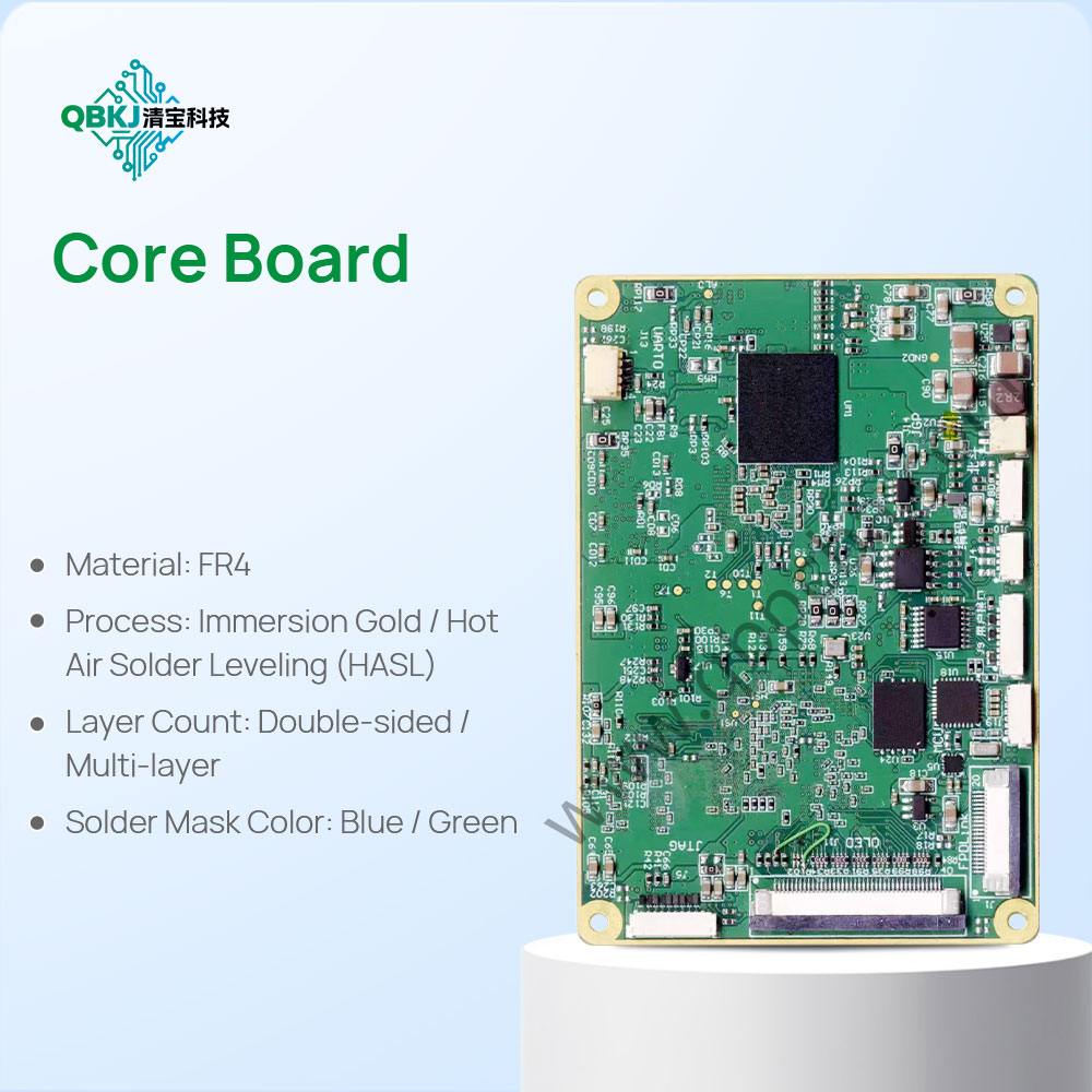
The process begins with Assembly-Level Documentation: The PCBA’s overall dimensions, component placement (X/Y/Z coordinates), and orientation (e.g., diode polarity, IC pin 1 alignment) are captured using 3D optical scanners and high-resolution cameras. A bill of materials (BOM) is created, documenting each component’s part number, manufacturer, package type, value, and quantity—cross-referenced with datasheets to ensure accuracy. Solder joint quality (e.g., fillet shape, absence of bridging) is documented via visual inspection and X-ray imaging for hidden joints (e.g., BGA).
Next is Electrical Documentation: The PCBA’s schematic diagram is reconstructed (via reverse PCBA schematic) and included, along with signal path diagrams, power distribution networks (e.g., 5V, 3.3V rails), and test points. Functional test procedures are documented—including input/output parameters (e.g., “Sensor input: 0-5V”, “Motor output: 12V DC”) and pass/fail criteria—based on testing the original PCBA’s performance with oscilloscopes, multimeters, and functional test fixtures.
Then comes Functional & Environmental Documentation: The PCBA’s operating parameters (temperature range, voltage tolerance, power consumption) are measured and recorded. Environmental compliance data (e.g., RoHS, REACH) is documented by verifying component materials and PCB finishes. For specialized applications (e.g., aerospace), additional records like vibration test results or radiation hardening specifications are included if applicable.
Finally, Document Validation & Compilation: All documents—BOM, schematic, component placement map, test procedures, and material specifications—are cross-checked against the physical PCBA to ensure accuracy. They are organized into a searchable database or document management system, using standard formats (e.g., PDF, Excel, CAD files) for accessibility. Challenges include documenting custom or proprietary components with limited datasheets and reconstructing functional test procedures for complex PCBAs. This process is vital for ensuring consistent repairs, enabling PCBA replication, and meeting regulatory requirements (e.g., FDA documentation for medical devices).
Email: 1330695973@qq.com
Factory: Room 703, Kelunte R&D Building, No. 1 Ganli 5th Road, Jihua Street, Longgang District, Shenzhen City