CN
-
Service Hotline
15766086363


Release Date:Mar 12, 2026
PCBA Clone Fabrication Process is the end-to-end workflow of creating exact functional replicas (clones) of a target Printed Circuit Board Assembly (PCBA) by integrating precise PCB cloning, component matching, automated assembly, and rigorous validation—ensuring the cloned PCBA is indistinguishable from the original in form, fit, and function. Unlike standard PCBA fabrication (relying on original design files), this process addresses scenarios where original documents are lost or obsolete, making it critical for replacing legacy PCBAs in aerospace, medical, or industrial control systems where performance consistency is non-negotiable.
The process begins with Original PCBA Forensics: Technicians use 3D laser scanners (with ±5μm accuracy) to capture component positions (X/Y/Z coordinates) and orientations (e.g., IC pin 1 alignment, diode polarity). High-resolution X-ray imaging documents hidden details like BGA solder ball geometry and inner-layer trace connections. A “golden sample” of the original PCBA is designated for side-by-side comparison throughout fabrication.
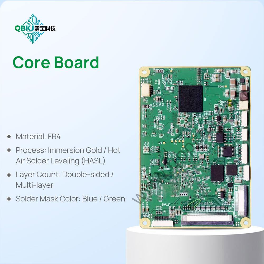
Next is PCB Clone Fabrication: The original PCB’s design is reverse-engineered—layer stackups (via X-ray tomography), trace routing, and via specifications are mapped to generate Gerber and drill files. Bare PCBs are fabricated using materials identical to the original (e.g., FR-4 substrate with 1oz copper, ENIG surface finish) and tested for impedance (matching high-speed signal requirements) and continuity (no open/short circuits) to ensure they mirror the original’s electrical properties.
Component sourcing is a critical step: Matching & Validation: Each component is cross-referenced via part number, manufacturer, and date code to source exact equivalents. Obsolete parts are replaced only with NOS (New Old Stock) components to maintain performance consistency. Components are tested individually (e.g., multimeters for resistors, oscilloscopes for microcontrollers) and in-circuit (to verify signal interactions) before assembly.
Assembly proceeds with Automated Precision: Cloned PCBs are loaded into SMT machines calibrated to the 3D-scanned coordinates, placing components with ±0.02mm alignment. Solder paste (same alloy as the original, e.g., Sn63/Pb37 or Pb-free SAC305) is applied via stencil, and reflow ovens use profiles matched to the original to ensure solder joint integrity. Through-hole components are soldered via wave soldering or certified manual processes.
Finally, Multi-Stage Validation: Cloned PCBAs undergo AOI (Automated Optical Inspection) for component misplacement, X-ray for BGA solder quality, functional testing (applying original input signals to confirm output matching), and environmental cycling (temperature/humidity) to replicate field conditions. Only PCBAs passing all tests—with performance metrics identical to the golden sample—are approved. Challenges include replicating custom ASICs (requiring specialized testing) and matching aging-related component characteristics (e.g., capacitor ESR) in legacy systems. This process delivers reliable, identical PCBA clones for mission-critical applications.
Email: 1330695973@qq.com
Factory: Room 703, Kelunte R&D Building, No. 1 Ganli 5th Road, Jihua Street, Longgang District, Shenzhen City