CN
-
Service Hotline
15766086363


Release Date:Mar 13, 2026
PCB Manufacturing from Copy is the process of producing bare PCBs using design data extracted from an existing “copy” PCB (a previously reversed or cloned board) — streamlining production by leveraging validated reversed design files while ensuring consistency with the original target PCB. Unlike direct reverse engineering from the original PCB (which requires extensive forensics), this process uses a pre-validated copy as the reference, reducing lead times and minimizing errors—ideal for scaling production of legacy PCBs or replenishing inventory for long-life products (e.g., industrial sensors, automotive infotainment modules).
The process starts with Copy PCB Validation: The reference copy PCB is inspected to confirm it matches the original target’s specifications—physical dimensions (via calipers), layer count (X-ray), and electrical performance (impedance testing). Any deviations (e.g., trace width variations) are corrected in the design files to ensure alignment with the original’s requirements.
Next is Design File Optimization: The reversed Gerber, drill, and layer stackup files from the copy PCB are refined for manufacturing scalability. DFM (Design for Manufacturing) checks are performed to optimize trace spacing (for etching efficiency), via placement (for drilling accuracy), and solder mask coverage (for consistency). For high-volume production, files are adjusted to accommodate standard manufacturing tolerances (e.g., ±0.1mm for trace width) without compromising alignment with the original.
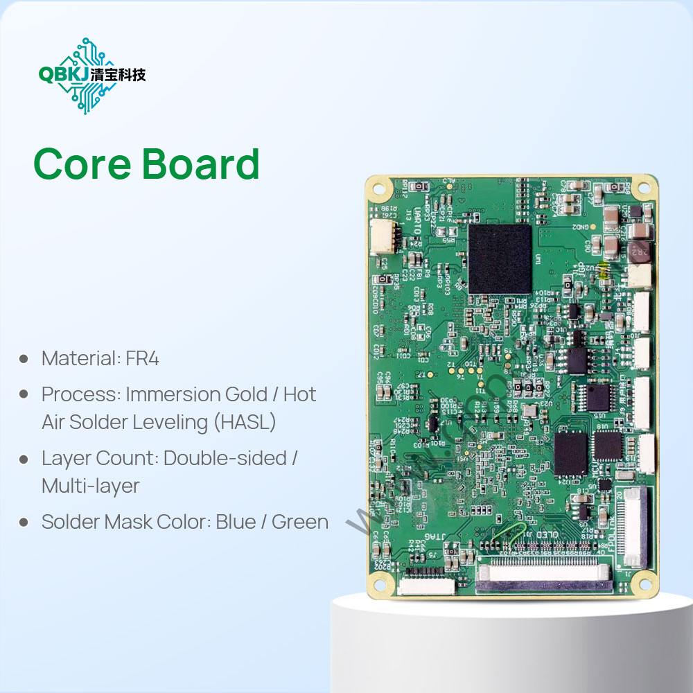
Material sourcing follows Original Specification Matching: Substrate material (e.g., FR-4 for standard use, Rogers 4350 for high-frequency PCBs), copper thickness (1oz/2oz), and surface finish (HASL, ENIG, or OSP) are selected to match both the copy PCB and the original target. Material certificates are verified to ensure compliance with industry standards (e.g., IPC-4101 for substrates) and application requirements (e.g., UL94 V-0 flame retardancy).
Manufacturing proceeds with Automated Production: PCBs are fabricated in batches using automated equipment—CNC routers cut substrates, laser direct imaging (LDI) transfers trace patterns (replacing traditional photomasks for higher accuracy), and chemical etching removes excess copper. Vias are drilled via CNC machines (with X-ray alignment to ensure position accuracy) and plated with copper to ensure conductivity. Surface finish is applied via automated lines, with thickness monitored via X-ray fluorescence (XRF) testing.
Quality control is integrated at every stage: In-Line Testing: Each batch undergoes AOI (for trace defects), impedance testing (for signal integrity), and continuity testing (for via connections). A sample from each batch is cross-compared to the copy PCB and original target to confirm consistency. Challenges include maintaining material consistency across batches (e.g., substrate dielectric constant) and adapting reversed files to newer manufacturing equipment (without altering critical dimensions). This process ensures cost-effective, consistent PCB production from validated copies.
Email: 1330695973@qq.com
Factory: Room 703, Kelunte R&D Building, No. 1 Ganli 5th Road, Jihua Street, Longgang District, Shenzhen City