CN
-
Service Hotline
15766086363


Release Date:Mar 16, 2026
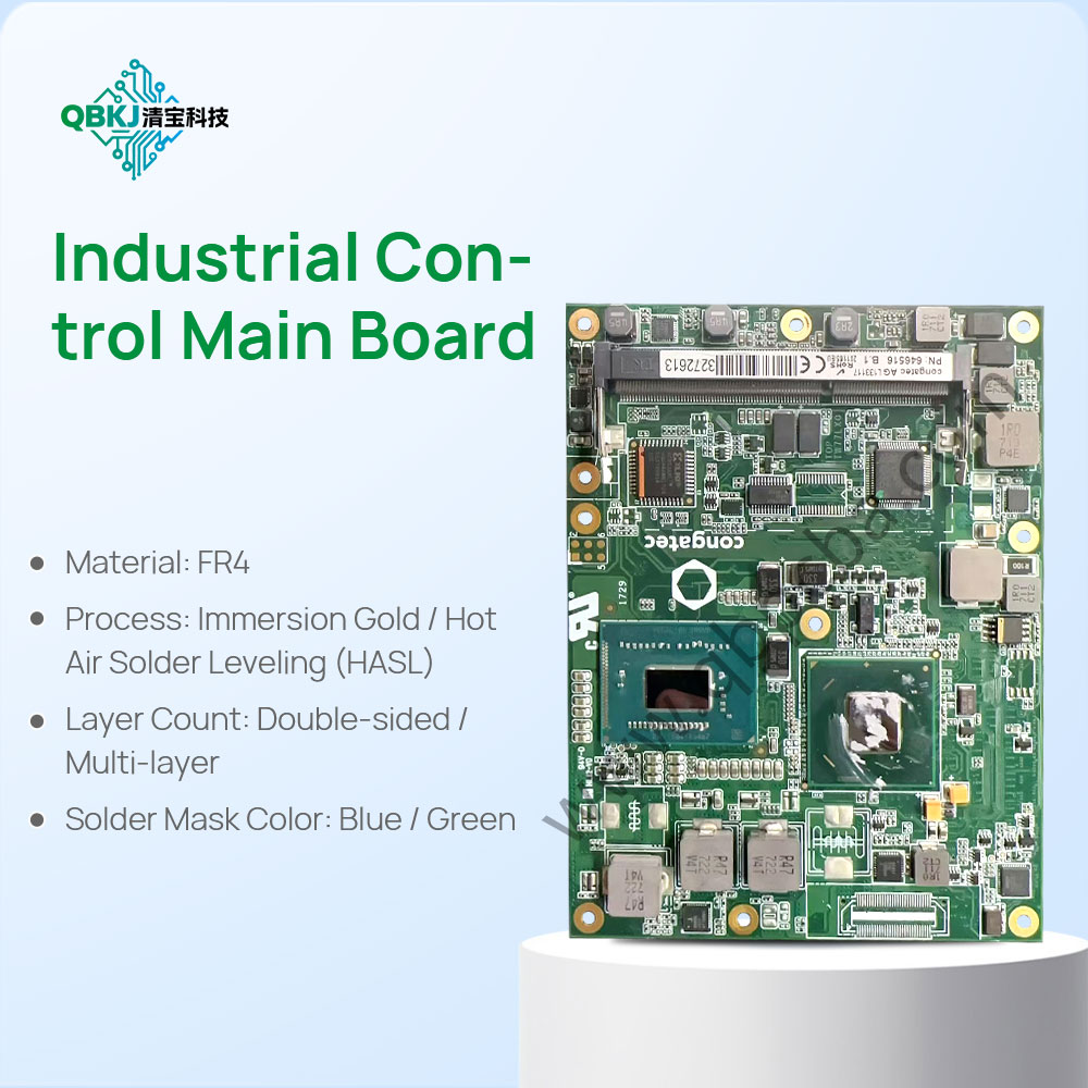
A PCB Copy Production Line is a dedicated, semi-automated/automated workflow designed to manufacture identical bare PCB copies in medium batches (50–500 units) using reverse-engineered design data—optimized for consistency, cost efficiency, and scalability while maintaining alignment with the original target PCB’s specifications. Unlike one-off PCB cloning (relying on manual processes), this line streamlines repeatable steps (e.g., imaging, etching, drilling) to reduce lead times and minimize human error. It is ideal for businesses needing regular replenishment of legacy PCBs (e.g., industrial controllers, medical device components) or medium-volume production of proven designs where original files are unavailable.
The line begins with Design Data Integration: Reverse-engineered Gerber, drill, and layer stackup files (from the original PCB) are loaded into the line’s MES (Manufacturing Execution System). The MES cross-references files with the original PCB’s digital twin (3D scan + electrical specs) to set equipment parameters—e.g., etching time, drill speed, and surface finish thickness.
Material handling is standardized: Substrate Preparation: Raw substrates (matched to the original’s material, e.g., FR-4, Rogers) are cut to size via CNC routers and inspected for defects (e.g., warping) before entering the line. Copper-clad substrates are cleaned to remove dust or oxidation, ensuring adhesion for trace patterns.
Core processing stations include: Imaging: Laser Direct Imaging (LDI) machines transfer reversed trace patterns onto copper layers—replacing traditional photomasks for faster setup and higher accuracy (±5μm). Etching: Automated chemical baths remove excess copper, with real-time monitoring (via optical sensors) to ensure trace width compliance (e.g., 0.2mm ±0.01mm). Drilling: CNC drill machines (equipped with X-ray alignment) create vias and mounting holes per reversed drill files, with hole size verified via laser micrometers. Plating: Electroless copper plating coats vias to ensure conductivity, followed by electrolytic plating to build copper thickness (matched to the original’s 1oz/2oz specification). Surface Finishing: Automated lines apply ENIG, HASL, or OSP finishes, with X-ray fluorescence (XRF) testing to confirm thickness (e.g., 50μm nickel, 1μm gold for ENIG).
Quality control is integrated at every stage: In-Line Inspection: After imaging/etching, AOI (Automated Optical Inspection) detects trace defects (e.g., nicks, bridging). Post-drilling, X-ray scanners verify hole position and via integrity. End-of-line testing includes continuity checks (via probe cards) and impedance testing (for high-frequency PCBs). Failed PCBs are diverted for rework or disposal, with root-cause analysis feeding back to the MES to optimize parameters.
Challenges include maintaining material consistency across batches (e.g., substrate dielectric constant) and adapting reversed files to line capabilities (e.g., adjusting drill speeds for hard substrates). This line ensures reliable, medium-volume PCB copy production with consistent quality.
Email: 1330695973@qq.com
Factory: Room 703, Kelunte R&D Building, No. 1 Ganli 5th Road, Jihua Street, Longgang District, Shenzhen City