CN
-
Service Hotline
15766086363


Release Date:Sep 08, 2026
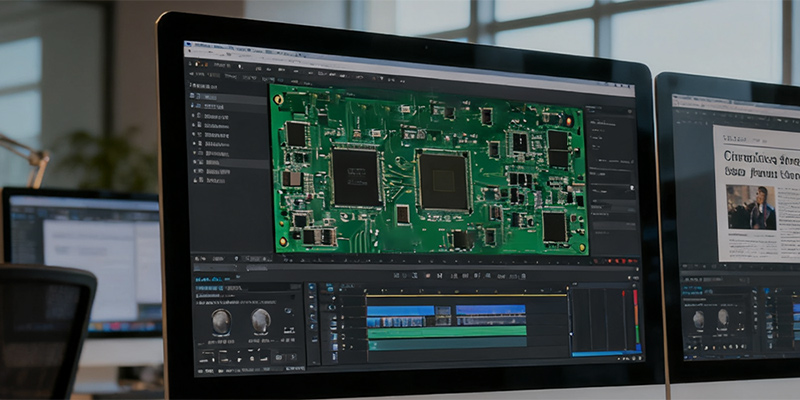
PCB clone solder mask file generation is a key process related to PCB surface protection, welding quality and circuit reliability, and the solder mask layer (green oil layer) is the most important protective layer on the PCB surface. The solder mask file accurately defines the coverage area of the solder mask ink on the PCB, including full-board ink coverage area, pad window opening area, test point window area, and partial ink removal area for heat dissipation and welding. Accurate solder mask file restoration and generation can ensure that the cloned PCB has the same anti-oxidation, anti-corrosion, insulation and solder resistance performance as the original board, effectively preventing circuit short circuits caused by tin bridging during welding, and improving the service life and environmental adaptability of the circuit board.
The solder mask file generation is based on the reverse analysis of the original PCB surface process. Technicians observe and detect the surface solder mask distribution characteristics of the original PCB through industrial microscopes, accurately distinguishing the solder mask covered area and the exposed copper window area. All pad positions of SMD and plug-in components, test point positions, and grounding copper foil contact positions that need tin coating are marked as window opening areas, while the wiring area, internal copper foil area, and non-welding structural area are marked as solder mask coverage areas. For special process designs such as partial ink removal for high-power device heat dissipation and solder mask bridging protection between fine-pitch pads, accurate feature extraction is carried out to completely retain the original board's process design logic.
In the data sorting and editing stage, professional PCB design software is used for precise drawing and optimization of the solder mask layer. The solder mask window size is calibrated one by one according to the pad size of the original board. The window opening tolerance is set in accordance with industrial standards to ensure that the window edge is completely fitted with the pad edge, without excessive window opening leading to exposed redundant copper foil, or too small window opening leading to pad ink covering and welding failure. For dense pin areas of IC chips, the solder mask bridge width is optimized to ensure that the insulation bridge between adjacent pads meets the process requirements, avoiding tin connection and short circuit during SMT welding. At the same time, the overall uniformity of the solder mask layer is adjusted, and redundant window openings and invalid coverage areas are cleaned up to standardize the entire layer data.
After the completion of editing, process verification and format export are carried out. The generated solder mask file is superimposed and compared with the wiring layer, pad layer and silk screen layer to check for layer interference and data errors, ensuring that the solder mask design does not affect circuit conduction, component welding and functional testing. Meanwhile, the solder mask process parameters are matched with the original board, including ink thickness, window opening accuracy and surface flatness standards. Finally, the standard Gerber format solder mask file is exported, which supports PCB factory screen printing, inkjet printing and photosensitive solder mask processes. The generated solder mask file ensures that the surface protection performance, welding manufacturability and appearance effect of the cloned PCB are consistent with the original sample, providing a reliable guarantee for the stable operation and long-term use of the circuit board.

Email: 15361682656@163.com
Factory: Room 703, Kelunte R&D Building, No. 1 Ganli 5th Road, Jihua Street, Longgang District, Shenzhen City