CN
-
Service Hotline
15766086363


Release Date:Sep 08, 2026
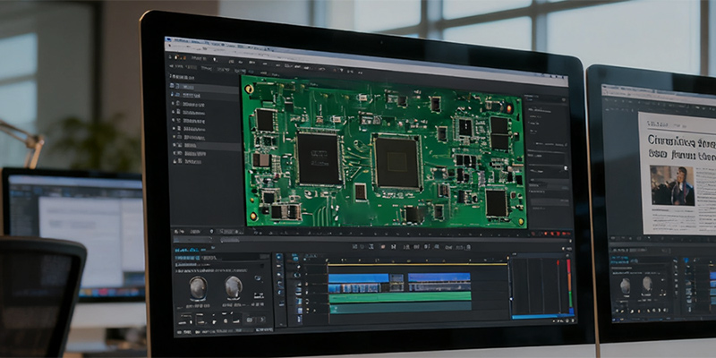
PCB reverse engineering silkscreen layer file restoration is an important part of PCB appearance and functional identification data reconstruction, which is responsible for accurately restoring all silkscreen pattern information on the original PCB surface, including component reference numbers, component polarity marks, circuit function labels, board model numbers, manufacturer logos, warning marks, and positioning identification patterns. The silkscreen layer is the visual identification layer of PCB products, which plays a key role in component assembly, subsequent maintenance, circuit debugging, and product identification. High-precision silkscreen layer restoration can ensure that the appearance of cloned PCBs is completely consistent with the original board, and the identification information is accurate and error-free, avoiding assembly confusion and maintenance difficulties caused by incorrect silkscreen information.
The silkscreen layer restoration process starts with high-definition image acquisition and feature extraction. Professional high-resolution industrial cameras and microscopic scanning equipment are used to perform ultra-clear shooting and scanning on the top and bottom silkscreen layers of the original PCB. For small-sized silk screen characters and tiny identification patterns on high-density PCBs, microscopic amplification scanning is adopted to capture the stroke details, size, position, and orientation of all silkscreen content. Technicians classify and sort all silkscreen elements, including alphabetic and numeric component labels (R, C, L, U, Q, J, etc.), positive and negative polarity marks of electrolytic components, pin sequence identification marks of integrated circuits, functional area division marks, product model specifications, and factory trademark patterns, to ensure that all silkscreen features of the original board are fully recorded.
The core link of restoration is vector redrawing and position calibration of silkscreen patterns. The original scanned bitmap silkscreen data is a raster image with fuzzy edges and easy distortion, which cannot be directly used for production. Therefore, technicians carry out one-by-one vector redrawing of all silkscreen content to convert fuzzy bitmap patterns into clear, smooth, and editable vector lines. During the redrawing process, the font size, stroke thickness, character spacing, and pattern proportion of the original silkscreen are strictly restored. At the same time, the relative position of each silkscreen label and the corresponding component pad is accurately calibrated to ensure that the silkscreen text is centered and positioned correctly, without offset, overlap, or deviation from the component position. For special irregular patterns and personalized logo marks, proportional restoration and detail optimization are carried out to retain the unique appearance features of the original board.
The final stage is silkscreen layer standardization processing and compatibility detection. After completing vector redrawing, the silkscreen layer is optimized according to PCB silk screen printing process specifications, removing redundant lines, broken strokes, and overlapping patterns, adjusting the silkscreen line width to meet the minimum process width requirements of screen printing and inkjet printing, avoiding silkscreen blurring, missing printing, and broken lines in production. Meanwhile, the silkscreen layer and other functional layers (solder mask layer, wiring layer, pad layer) are checked for interference to ensure that the silkscreen content does not cover functional pads and test points, which would affect component welding and circuit testing. The restored silkscreen layer file is exported in standard Gerber format, which is compatible with all PCB production equipment. The complete silkscreen layer data ensures that the appearance identification, assembly guidance, and product consistency of the cloned PCB are completely consistent with the original sample, meeting the appearance quality and functional use requirements of industrial products.

Email: 15361682656@163.com
Factory: Room 703, Kelunte R&D Building, No. 1 Ganli 5th Road, Jihua Street, Longgang District, Shenzhen City