CN
-
Service Hotline
15766086363


Release Date:Oct 26, 2026
Thin PCB clone and ultra thin circuit board copy services address one of the most challenging areas of reverse engineering because mechanical fragility, layer registration, and handling constraints dominate the process. Ultra thin boards are commonly defined as PCBs with an overall thickness below 1.0 mm, and many advanced designs fall in the 0.4 mm to 0.8 mm range. Some flexible and rigidflex boards are even thinner, occasionally reaching 0.2 mm or less. Cloning such boards requires specialized fixtures, lowstress imaging methods, and precise control of lamination and drilling. The goal is to reproduce the original electrical function while preserving the mechanical flexibility, bend radius, and dimensional stability that the application demands.
The reverse engineering phase of a thin PCB clone begins with careful sample preparation. Because thin boards warp easily, they must be mounted on rigid carriers before scanning, Xray inspection, or crosssectioning. Layer counts are identified through Xray and microsectioning, and copper thickness is measured using metallographic methods. Ultra thin boards often use very thin copper foils, sometimes 9 μm or 12 μm, which makes trace repair and rework extremely delicate. The cloning engineer must also determine whether the original uses FR4, polyimide, BT resin, or a specialty material. Polyimide is common in thin and flexible designs because of its thermal stability and mechanical strength, while FR4 remains popular for costsensitive rigid thin boards.
Stackup reconstruction in ultra thin circuit board copy is a balancing act. Fewer layers may be used to reduce thickness, but this can force denser routing and tighter impedance control. Conversely, some designs use many thin layers to achieve high density while keeping overall thickness low. The clone must replicate prepreg types, resin content, and lamination parameters to avoid delamination, resin starvation, or excessive warp. Registration between layers becomes more difficult as thickness decreases, because the ratio of drill depth to board thickness changes and small misalignments can cause shorts or opens. Laser drilling is often required for microvias, and plasma desmear may be needed to clean highaspectratio holes without damaging thin dielectrics.
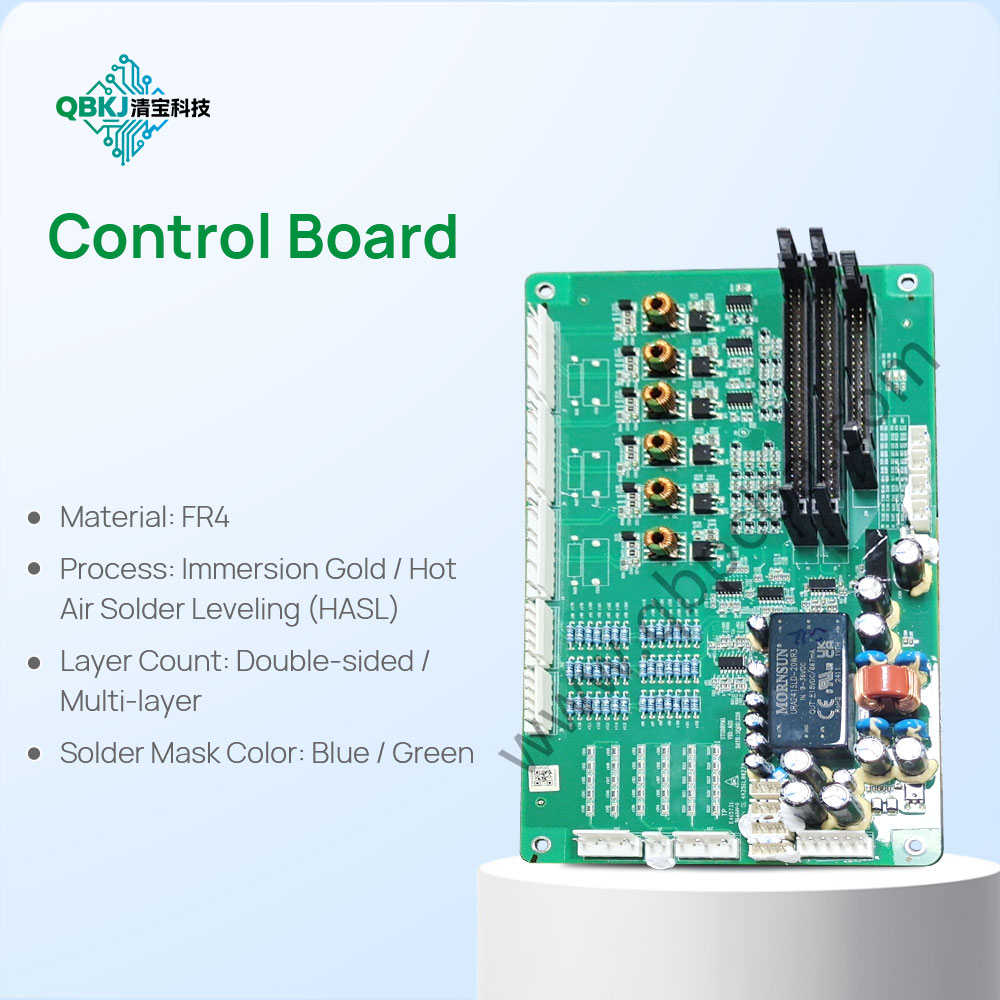
Surface finish selection is equally important for thin boards. HASL can introduce thermal stress and uneven thickness, which may warp ultra thin substrates. Immersion gold, immersion silver, OSP, and electroless nickel immersion gold are generally preferred because they are flat and lowstress. For flexible and rigidflex clones, coverlay or soldermask selection affects bend performance and adhesion. The cloning service must also consider panelization and handling: thin boards often require carrier panels, stiffeners, or tapeandreel packaging to survive assembly. Final verification includes dimensional inspection, electrical continuity and isolation testing, impedance measurement where applicable, and functional testing under the intended bend or flex conditions. A qualified thin PCB clone provider should supply a complete documentation package, including stackup drawings, material certificates, test reports, and recommendations for assembly handling.

Email: 15361682656@163.com
Factory: Room 703, Kelunte R&D Building, No. 1 Ganli 5th Road, Jihua Street, Longgang District, Shenzhen City