CN
-
Service Hotline
15766086363


Release Date:Sep 07, 2026
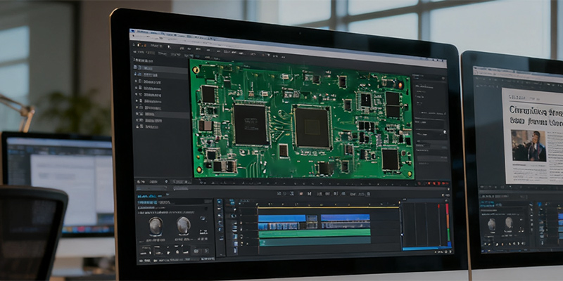
PCB clone 3D model file output is an indispensable technical link in modern high-precision PCB cloning and electronic product structural design, which realizes the three-dimensional digital restoration of the entire circuit board through precise data collection, modeling reconstruction, and parameter optimization of physical PCB samples. Different from traditional 2D PCB layout files, 3D model files can truly restore the spatial structure, component height distribution, board body thickness, hole position height, and three-dimensional spacing of the original PCB, providing accurate data support for product structural matching, shell design, mechanical interference detection, and virtual assembly simulation. This technology is widely applied in consumer electronics, industrial control equipment, automotive electronics, aerospace equipment, and medical electronic product cloning and secondary development, effectively solving the structural adaptation problems caused by inconsistent spatial dimensions in traditional 2D cloning.
The 3D model reconstruction process of PCB cloning starts with full-board high-precision data acquisition. Professional 3D scanners and high-resolution industrial cameras are used to perform omnidirectional scanning and image acquisition on the original PCB, including board outline dimensions, board thickness, cutting groove position, positioning hole distribution, component installation position, component body height, pin protrusion height, and the three-dimensional spatial distance between adjacent components. For high-density PCBs with BGA, QFN, and fine-pitch ICs, ultra-high-precision scanning is adopted to capture tiny spatial features such as solder ball height and chip body indentation, ensuring that the collected 3D data is completely consistent with the physical board. At the same time, 2D layout data obtained by reverse scanning is combined to calibrate the plane coordinate position of each component, realizing the precise matching of 2D layout coordinates and 3D spatial dimensions.
The core link of 3D model output is hierarchical modeling and structural restoration. Technicians split the PCB 3D model into multiple independent modeling units according to structural layers, including PCB substrate model, copper foil wiring layer model, solder mask layer model, silk screen layer model, through-hole and via hole model, and all component 3D entity models. The PCB substrate is modeled with accurate thickness, outline radian, and edge cutting process parameters; the internal wiring and copper foil areas are restored in real thickness and spatial position; each electronic component is matched with a standard or customized 3D model package according to its actual size, and the height, orientation, and installation offset of each component are calibrated one by one. For special structural components such as plug-in connectors, adjustable capacitors, and shielding covers, independent customized 3D modeling is carried out to restore their unique spatial structures and movable characteristics.
After the completion of preliminary modeling, model optimization, format conversion, and precision verification are carried out. The initial 3D model is optimized for details such as surface flatness, hole wall smoothness, and component assembly gap to eliminate model distortion, spatial overlap, and dimensional deviation caused by scanning errors. Meanwhile, multiple mainstream 3D file formats are exported according to customer needs, including STEP, STL, 3DS, and Altium 3D native formats, which are compatible with mainstream 3D design software such as SolidWorks, UG, Pro/E, and AutoCAD. Finally, virtual assembly simulation and dimensional comparison verification are performed between the 3D model and the original physical PCB to ensure that the overall outline error is controlled within ±0.02mm and the component spatial position error is within ±0.01mm. The final output 3D model file can be directly used for product shell design, mechanical interference check, production fixture design, and product virtual display, greatly improving the overall matching accuracy and production yield of cloned PCB products.

Email: 15361682656@163.com
Factory: Room 703, Kelunte R&D Building, No. 1 Ganli 5th Road, Jihua Street, Longgang District, Shenzhen City