CN
-
Service Hotline
15766086363


Release Date:Mar 11, 2026
The PCB Copy Manufacturing Process is the end-to-end workflow of producing identical physical replicas of a target PCB using design data extracted via reverse engineering—from initial reverse engineering of the original board to final fabrication and quality testing of copied PCBs. Unlike standard PCB manufacturing (which starts with original Gerber files), this process relies on reversed design data to replicate PCBs when original documents are lost, obsolete, or unavailable, making it essential for replacing legacy PCBs (e.g., in industrial controllers, military equipment) or scaling production of proven designs.
The process begins with Original PCB Reverse Engineering: Technicians document the original PCB’s physical attributes (dimensions, layer count) using calipers and 3D scanners. For multi-layer PCBs, X-ray tomography or chemical etching exposes inner layers, while high-resolution cameras capture trace details (width, spacing) and component footprints. This data is converted into editable files—including Gerber files (for fabrication), drill files (for vias and mounting holes), and a bill of footprints (BOF)—via specialized software (e.g., Altium, KiCad).
Next is Design Validation: The reversed Gerber files are cross-checked against the original PCB to ensure accuracy. Overlay analysis (comparing digital files to scanned images of the original) verifies trace alignment and pad sizes, while DFM checks confirm compliance with manufacturing standards (e.g., IPC-2221 for trace width, IPC-6012 for PCB quality). Adjustments are made for discrepancies—e.g., resizing a via that’s 0.1mm too small in the reversed file.
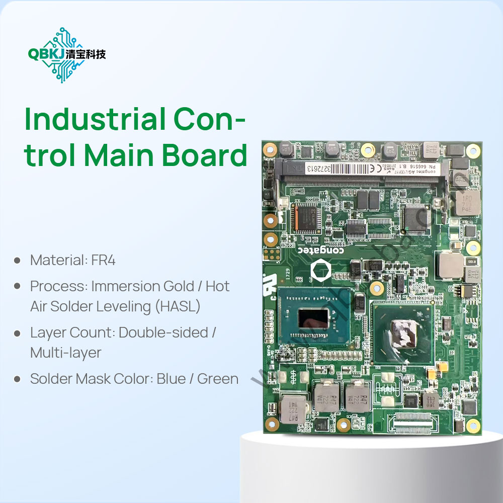
Then comes Material Sourcing: Materials matching the original PCB are procured—substrate (e.g., FR-4 for standard applications, Rogers for high-frequency designs), copper cladding (e.g., 1oz for low-current circuits, 2oz for power circuits), and surface finish (e.g., ENIG for corrosion resistance, HASL for cost-effectiveness). Material testing (e.g., dielectric strength for substrates) ensures consistency with the original’s performance.
Fabrication follows standard PCB manufacturing steps but uses reversed data: Substrate Preparation (cutting to size), Copper Lamination (applying copper sheets), Photolithography (transferring reversed trace patterns to copper via UV light), Etching (removing excess copper to leave traces), Drilling (creating vias/mounting holes using reversed drill files), Plating (coating holes with copper for conductivity), and Surface Finishing (applying ENIG/HASL).
Finally, Quality Testing: Copied PCBs undergo rigorous inspection—AOI (Automated Optical Inspection) for trace defects, X-ray for via integrity, continuity testing for open/short circuits, and impedance testing for signal performance. Only PCBs matching the original’s specifications are approved for use. Challenges include replicating obsolete materials (e.g., discontinued substrates) and maintaining tight tolerances for high-density PCBs (e.g., 0.4mm pitch BGA footprints). This process ensures consistent, reliable PCB copies for critical applications where original manufacturing is no longer feasible.
Email: 1330695973@qq.com
Factory: Room 703, Kelunte R&D Building, No. 1 Ganli 5th Road, Jihua Street, Longgang District, Shenzhen City