CN
-
Service Hotline
15766086363


Release Date:Mar 16, 2026
The PCB Clone and Testing Process is a systematic workflow to create identical bare PCB replicas and validate their electrical, physical, and functional compliance with the original target PCB—combining precise cloning with rigorous testing to ensure reliability. Unlike PCB cloning alone (focused on replication), this process prioritizes verification at every stage, making it critical for applications where PCB performance directly impacts system functionality (e.g., aerospace avionics, medical devices, high-frequency communication systems).
The process begins with Original PCB Reverse Engineering: Technicians use high-resolution cameras and 3D scanners to capture physical dimensions (length, width, thickness) and component footprints. For multi-layer PCBs, X-ray tomography (non-destructive) maps inner layers, trace routing, and via positions. This data is converted into Gerber files, drill files, and a layer stackup report—cross-referenced with IPC standards (e.g., IPC-2221 for trace width) to ensure design accuracy.
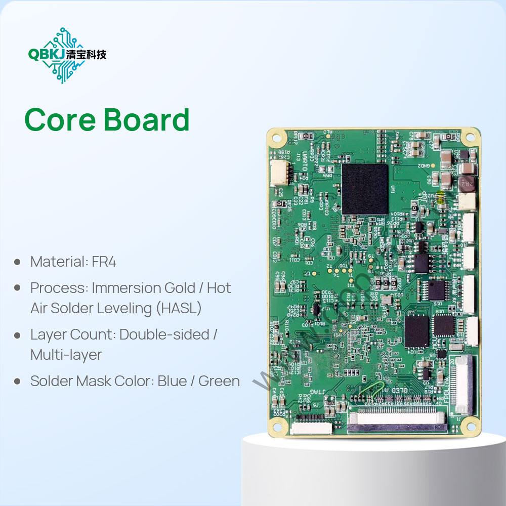
Next is PCB Clone Fabrication: Bare PCBs are manufactured in small batches using materials matched to the original (e.g., FR-4 substrate, 1oz copper, ENIG surface finish). Fabrication steps include substrate cutting, copper lamination, laser imaging (trace patterns), chemical etching, drilling, and plating. Each step is monitored to maintain tight tolerances—e.g., trace width ±0.01mm, via diameter ±0.02mm.
Testing begins with Physical & Visual Inspection: Cloned PCBs are inspected for physical alignment with the original—dimensions measured via calipers, mounting hole positions verified via coordinate measuring machines (CMMs), and surface finish checked via X-ray fluorescence (XRF) to confirm thickness (e.g., 50μm nickel for ENIG). AOI (Automated Optical Inspection) detects visual defects: trace nicks, bridging, solder mask bubbles, or missing silkscreen.
Electrical testing follows Performance Validation: Continuity testing uses a probe card to check for open circuits (e.g., broken traces, unplated vias) and short circuits (e.g., adjacent trace bridging). Impedance testing (via a vector network analyzer) verifies trace impedance matches the original—critical for high-speed signals (e.g., USB 3.0, PCIe) where impedance mismatches cause signal reflection. For multi-layer PCBs, time-domain reflectometry (TDR) maps signal propagation to ensure inner-layer trace integrity.
Environmental testing ensures Resilience: Cloned PCBs undergo thermal cycling (e.g., -55°C to 125°C for 100 cycles) to test material durability and via reliability. Humidity testing (85% RH, 85°C for 500 hours) assesses corrosion resistance of surface finishes. For high-reliability applications, mechanical stress testing (bending, vibration) simulates field conditions.
Finally, Compliance Verification: Cloned PCBs are tested against industry standards (e.g., IPC-6012 for PCB quality, UL94 V-0 for flame retardancy) and application-specific requirements (e.g., MIL-STD-202 for military use). A test report is compiled, documenting results and any deviations from the original—with failed clones analyzed for root causes (e.g., etching errors, material inconsistencies) and reworked or discarded.
Challenges include replicating obsolete materials (e.g., discontinued substrates) and validating high-frequency performance (e.g., 5G PCB clones). This process ensures cloned PCBs meet the original’s performance, reliability, and compliance standards.
Email: 1330695973@qq.com
Factory: Room 703, Kelunte R&D Building, No. 1 Ganli 5th Road, Jihua Street, Longgang District, Shenzhen City