CN
-
Service Hotline
15766086363


Release Date:Jan 26, 2026
Reverse PCB manufacturing is the end-to-end process of producing new PCBs using design data extracted through PCB reverse analysis, essentially reversing the traditional manufacturing workflow (which starts with design files and ends with a physical board). It begins with validating the reversed design: engineers cross-check the extracted schematic, Gerber files, and layer stackup against the original PCB to ensure accuracy—verifying details like trace width (to handle current loads), via size (for reliability), and dielectric material (for signal integrity).
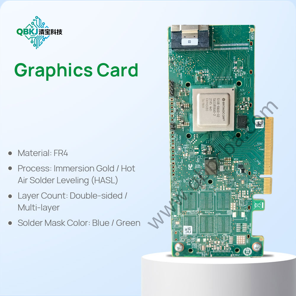
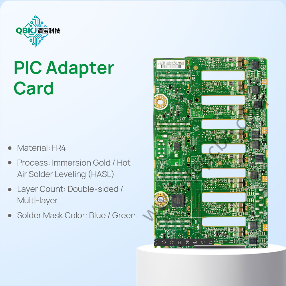
Next, the manufacturing process follows standard PCB production steps but uses reversed data: first, the substrate (usually FR-4) is cut to size; then, copper cladding is applied, and traces are etched using the reversed Gerber files (via photolithography). For multi-layer PCBs, layers are laminated together with dielectric material, and vias (drilled and plated) connect layers—all based on the reversed stackup data. After surface finishing (e.g., HASL or ENIG to prevent oxidation), the board undergoes quality testing: electrical tests (e.g., continuity checks) ensure no short circuits, while visual inspections verify trace accuracy. Reverse PCB manufacturing is critical for replacing legacy boards (e.g., in medical devices or aerospace equipment where original manufacturers no longer produce them) and scaling custom designs (once a reversed design is validated, it can be mass-produced). Key challenges include matching the original PCB’s material properties (e.g., thermal conductivity) and meeting strict manufacturing tolerances (especially for high-frequency PCBs), which require collaboration with specialized manufacturers.
Email: 1330695973@qq.com
Factory: Room 703, Kelunte R&D Building, No. 1 Ganli 5th Road, Jihua Street, Longgang District, Shenzhen City