CN
-
Service Hotline
15766086363


Release Date:Jan 22, 2026
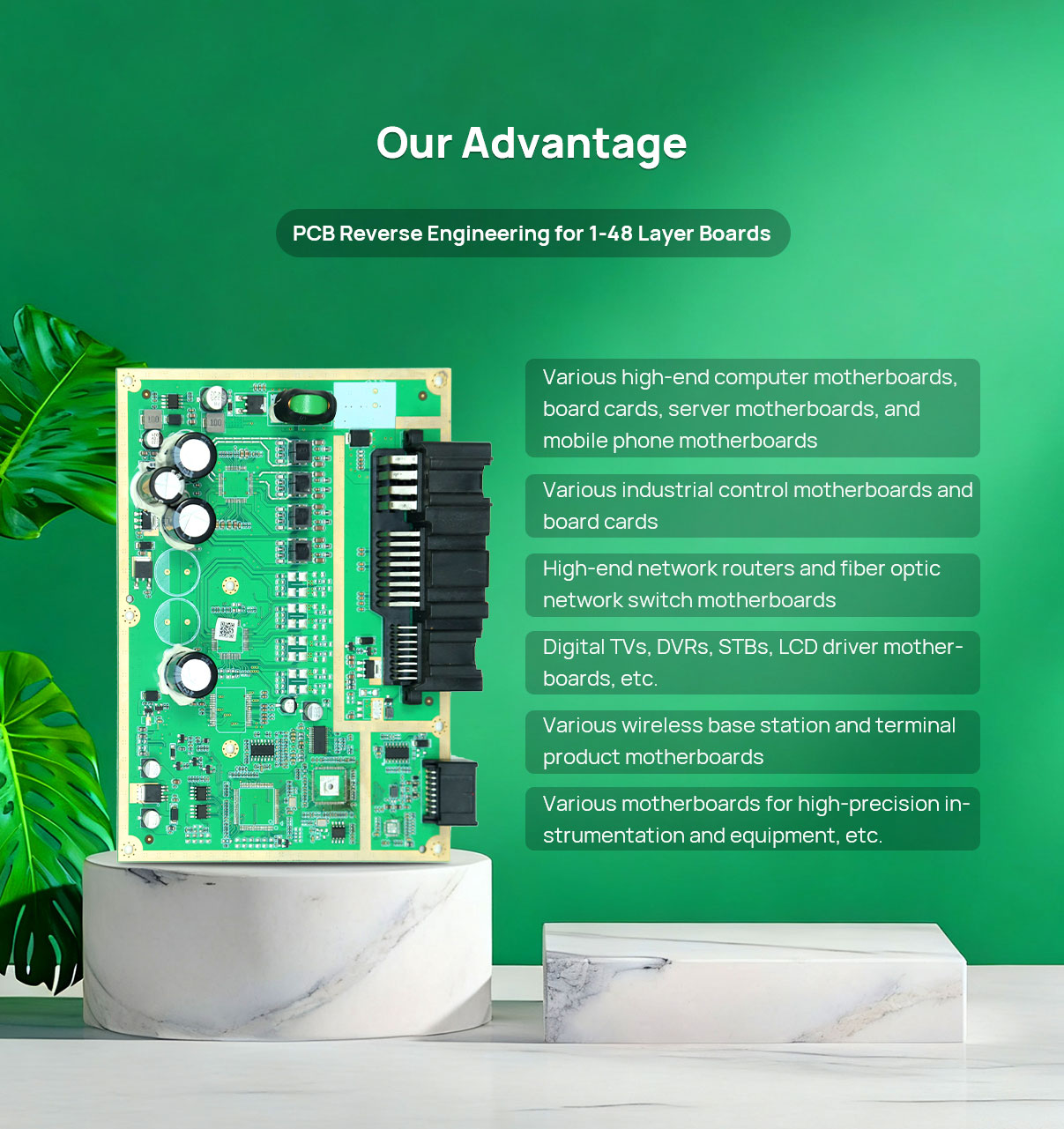
PCB reverse design is the technical process of reconstructing a digital design (schematic and layout files) from a physical bare printed circuit board (PCB)—with the goal of not just copying the design, but also understanding its logic, optimizing it, or adapting it to new requirements. Unlike reverse PCB clone (which focuses on physical replication), PCB reverse design emphasizes creating editable, scalable design files that can be modified for improved performance, cost reduction, or compatibility with new components.
The process begins with detailed data extraction: using 3D scanners and digital microscopes, technicians capture the PCB’s physical dimensions, trace routing, component footprints, and via locations. For multi-layer PCBs, X-ray machines or layer-peeling techniques map internal layers, and continuity testers verify electrical connections to build an initial netlist (a list of all electrical paths). This data is imported into PCB design software, where engineers reconstruct the schematic—labeling components, defining net names, and verifying circuit logic (e.g., ensuring a voltage regulator is correctly connected to power and ground).
Once the base schematic is complete, engineers refine the design for optimization: they may adjust trace widths to improve signal integrity (e.g., wider traces for high-current paths), relocate vias to reduce noise (critical for high-frequency PCBs), or replace obsolete component footprints with modern alternatives. For example, a reverse-designed industrial PCB might have its legacy DIP component footprints updated to SMT to reduce board size and assembly costs.
Validation involves fabricating a prototype from the reverse-designed files and testing it against the original PCB’s performance—measuring parameters like signal speed, power consumption, and thermal efficiency. Any discrepancies are addressed by refining the design. PCB reverse design is valuable for innovation (adapting legacy designs to new technologies) and cost savings (optimizing material usage), making it a key tool for industries like aerospace (upgrading avionics PCBs) and consumer electronics (redesigning outdated devices).
Email: 1330695973@qq.com
Factory: Room 703, Kelunte R&D Building, No. 1 Ganli 5th Road, Jihua Street, Longgang District, Shenzhen City