CN
-
Service Hotline
15766086363


Release Date:Jan 19, 2026
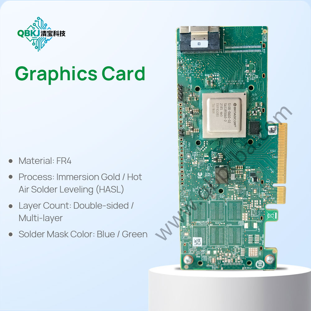
PCBA clone prototyping is the phase of creating small-batch, functional replicas of an original PCB to validate design accuracy, test functionality, and identify issues before full-scale production. This stage is critical for mitigating risks—even minor discrepancies in cloning (e.g., incorrect component placement, trace routing errors) can be corrected during prototyping, avoiding costly rework later.
The prototyping process starts with limited-scale fabrication: using the reconstructed schematic and layout from the cloning analysis, manufacturers produce 5–50 prototype PCBs (depending on testing needs). Component assembly follows, using the same parts (or validated equivalents) as the original, with manual or semi-automated assembly to ensure precision. Unlike mass production, prototyping prioritizes speed over volume, allowing for quick adjustments if issues arise.
Testing is the core of PCBA clone prototyping: prototypes undergo functional testing to verify they match the original’s performance (e.g., a cloned IoT prototype testing data transmission range). They also undergo fit testing to ensure compatibility with enclosures or adjacent components (e.g., a cloned smart home PCB fitting into a custom device case). If discrepancies are found—such as a sensor not communicating with the microcontroller—engineers debug the prototype by adjusting the layout, replacing components, or modifying firmware.
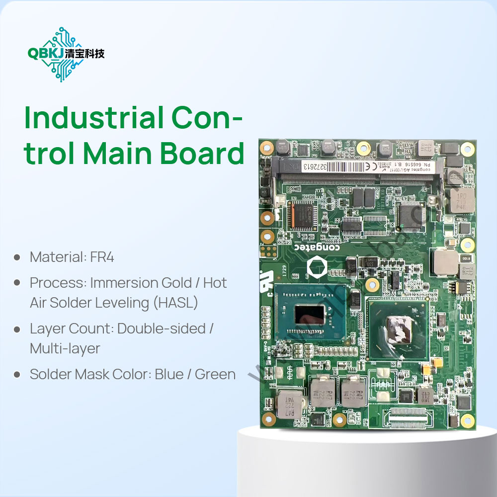
Once prototypes pass all tests, they serve as a “golden sample” for mass production, ensuring consistency across larger batches. For many use cases (e.g., legacy equipment replacement, startup product validation), prototyping is also used to gather user feedback—for example, a cloned industrial control board prototype tested by factory operators to confirm usability. PCBA clone prototyping bridges the gap between design and production, ensuring the final cloned PCBs are reliable and fit for purpose.
Email: 1330695973@qq.com
Factory: Room 703, Kelunte R&D Building, No. 1 Ganli 5th Road, Jihua Street, Longgang District, Shenzhen City