CN
-
Service Hotline
15766086363


Release Date:Apr 01, 2026
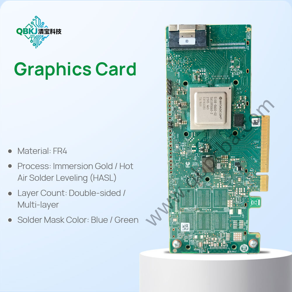
SMT (Surface Mount Technology) placement and PCBA (Printed Circuit Board Assembly) assembly are core processes in modern electronics manufacturing, widely used in the production of small appliances, consumer electronics, industrial equipment, medical devices, and other products. SMT placement is the process of mounting surface-mounted components (such as resistors, capacitors, diodes, integrated circuits, etc.) on the surface of the PCB (Printed Circuit Board) through automated equipment, and then forming a reliable electrical connection through reflow soldering. PCBA assembly processing is a comprehensive process that integrates SMT placement, through-hole insertion, soldering, testing, and other links, transforming the bare PCB and discrete components into a functional PCBA board. Our SMT placement + PCBA assembly processing service adopts advanced technology, automated equipment, and strict quality control, providing customers with high-efficiency, high-quality, and cost-effective assembly solutions to meet the diverse needs of mass production and small-batch customization.
The SMT placement process is the foundation of PCBA assembly, and its accuracy and efficiency directly affect the quality and production capacity of the final PCBA board. We have introduced a full set of advanced SMT production equipment, including high-precision solder paste printers, high-speed automated placement machines, reflow soldering ovens, and AOI (Automated Optical Inspection) equipment, to ensure the stability and consistency of the SMT placement process. The solder paste printer adopts a closed-loop control system with a printing accuracy of ±0.01mm, which can accurately apply the appropriate amount of solder paste to the PCB pads. The printer is equipped with a vision positioning system, which can automatically align the PCB and the stencil, avoiding printing deviations caused by PCB positioning errors. We also use high-quality stencils with precise opening sizes to ensure that the solder paste is evenly applied and the amount of solder paste is consistent, laying a good foundation for subsequent soldering.
The high-speed automated placement machine is the core equipment of the SMT placement process, and we have equipped multiple models of placement machines to meet the needs of different components and PCB sizes. Our placement machines have a placement speed of up to 50,000 components per hour, and can handle components of various sizes and types—from small 01005-sized resistors and capacitors to large integrated circuits (ICs), ball grid arrays (BGAs), and quad flat packages (QFPs). The placement machine adopts advanced vision positioning and laser alignment technology, with a placement accuracy of ±0.03mm, ensuring that each component is accurately placed on the PCB pad. The placement machine is also equipped with an automatic component feeding system, which can automatically feed components from the tape, tray, or tube, reducing manual operation and improving production efficiency. For special components (such as irregularly shaped components), we use customized fixtures and programming to ensure accurate placement.
After the SMT placement is completed, the PCB enters the reflow soldering stage, which is the key link to form a reliable solder joint. Our reflow soldering ovens adopt a multi-zone temperature control system (usually 8-12 zones), which can precisely control the temperature curve of the soldering process. The temperature curve is divided into four stages: preheating, soaking, reflow, and cooling. In the preheating stage, the temperature of the PCB and components is gradually raised to 150-180℃ to avoid thermal shock and damage to the components; in the soaking stage, the temperature is maintained at 180-200℃ for a certain period of time to activate the flux, remove the oxide layer on the surface of the pads and component pins, and ensure good wetting of the solder paste; in the reflow stage, the temperature is raised to the melting point of the solder paste (about 217℃ for lead-free solder paste), and the solder paste melts to form a dense solder joint; in the cooling stage, the temperature is rapidly reduced to room temperature, and the solder joint solidifies to form a stable intermetallic compound (IMC) layer, which enhances the mechanical strength and electrical conductivity of the solder joint. We optimize the temperature curve according to the type of solder paste, the size of the components, and the thickness of the PCB to ensure that each solder joint meets the highest quality standards.
In addition to SMT placement, PCBA assembly processing also includes through-hole insertion (THT) and wave soldering for components that cannot be surface-mounted, such as connectors, fuses, and transformers. We use automated through-hole insertion equipment to insert the component pins into the pre-drilled holes on the PCB, ensuring that the insertion depth and position are accurate. The wave soldering machine adopts a nitrogen-inerted wave soldering process, which can form a uniform and firm solder joint on the back of the PCB, avoiding soldering defects such as cold solder joints and solder bridges. For small-batch or special products, we also provide manual insertion and hand soldering services, with professional operators who have rich experience in soldering to ensure the quality of the solder joint.
Testing is an important part of SMT placement + PCBA assembly processing, and we have established a comprehensive testing system to ensure the quality of the PCBA board. The testing process includes solder paste inspection (SPI), pre-reflow AOI, post-reflow AOI, X-ray inspection, functional testing, and aging testing. SPI is used to detect the amount and uniformity of solder paste printing, avoiding defects caused by insufficient or excessive solder paste; pre-reflow AOI detects component placement errors (such as misalignment, missing components, and reversed polarity) before reflow soldering, reducing the cost of rework; post-reflow AOI detects soldering defects (such as cold solder joints, solder bridges, and missing solder) after reflow soldering; X-ray inspection is used to detect hidden solder joints (such as BGA and QFN components) to ensure the quality of internal solder joints; functional testing simulates the actual working environment of the PCBA board to test its functional performance; aging testing tests the long-term stability and reliability of the PCBA board. Only PCBA boards that pass all tests can enter the packaging and delivery stage.
We also pay attention to the optimization of the production process and cost control. By adopting automated production lines, we improve production efficiency, reduce human errors, and lower production costs; by optimizing the placement sequence and production scheduling, we reduce the production cycle and improve the utilization rate of equipment; by establishing long-term cooperative relationships with component suppliers, we obtain high-quality components at competitive prices, further reducing the cost of PCBA assembly. We also provide customized assembly solutions according to the specific needs of customers, whether it is mass production (with a daily production capacity of up to 100,000 pieces) or small-batch customization (minimum order quantity of 1 piece), we can flexibly adjust the production plan to meet the diverse needs of customers. With advanced technology, reliable equipment, strict quality control, and professional services, our SMT placement + PCBA assembly processing service has become a trusted choice for many customers, helping them improve product quality, reduce production costs, and accelerate product launch.
Email: 1330695973@qq.com
Factory: Room 703, Kelunte R&D Building, No. 1 Ganli 5th Road, Jihua Street, Longgang District, Shenzhen City