CN
-
Service Hotline
15766086363


Release Date:Mar 04, 2026
PCBA Circuit Duplication is the end-to-end process of creating an identical functional replica of a Printed Circuit Board Assembly (PCBA)—encompassing both the duplicated PCB (as in PCB circuit duplication) and the precise placement, soldering, and validation of all components. Unlike PCB duplication (which only copies the bare board), this ensures the final PCBA matches the original’s electrical performance, component interactions, and environmental resilience, making it ideal for replacing failed PCBAs in mission-critical systems (e.g., medical monitors, automotive infotainment).
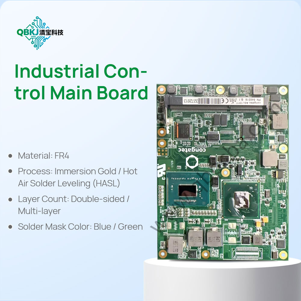
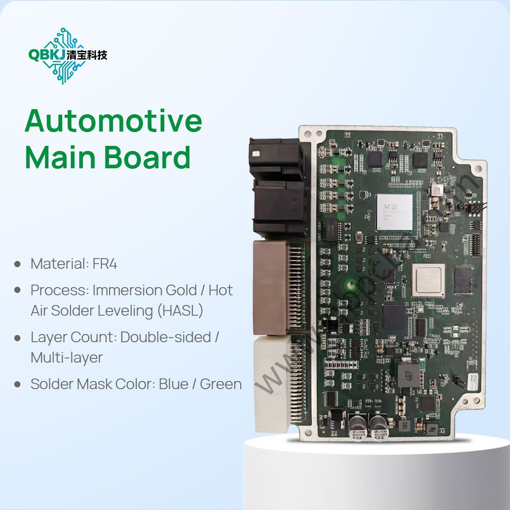
The process begins with Original PCBA Documentation: Technicians use 3D scanners and high-resolution cameras to capture component positions (X/Y/Z coordinates), orientations (e.g., diode polarity, IC pin 1 location), and solder joint profiles. A detailed BOM is created, with each component’s part number, manufacturer, package type (e.g., 0201 SMD, DIP-8), and electrical specifications (e.g., resistor tolerance, capacitor voltage rating) documented.
Next is PCB Duplication: As outlined in PCB circuit duplication, the original PCB’s circuit layout is replicated, with Gerber files generated and prototype PCBs fabricated. These PCBs are inspected to ensure they match the original’s physical and electrical properties (e.g., trace impedance, via conductivity).
Component sourcing is critical: Component Procurement & Validation: Identical components are sourced from authorized distributors; if obsolete, equivalents are selected by matching form (package size), fit (footprint compatibility), and function (electrical specs). Components are tested (via multimeters, component testers) to confirm they meet original performance standards.
Then comes Assembly: The duplicated PCBs are populated using automated SMT placement machines (for miniaturized components) or manual soldering (for through-hole parts), with solder paste type and reflow oven profiles matched to the original to ensure solder joint quality. Post-assembly, Inspection & Testing is conducted: AOI (Automated Optical Inspection) checks for component misplacement or solder defects; X-ray inspection verifies BGA solder ball integrity; and functional testing (applying input signals, measuring outputs) confirms the duplicated PCBA behaves identically to the original. Environmental testing (temperature cycling, humidity exposure) may also be performed for rugged applications.
Challenges include sourcing rare or obsolete components (requiring partnerships with specialty distributors), maintaining precise component placement (critical for high-speed PCBs), and ensuring long-term reliability (minor solder joint defects can cause premature failure). Legal and ethical compliance (verifying IP rights) is essential to avoid infringement.
Email: 1330695973@qq.com
Factory: Room 703, Kelunte R&D Building, No. 1 Ganli 5th Road, Jihua Street, Longgang District, Shenzhen City