CN
-
Service Hotline
15766086363


Release Date:Oct 20, 2026
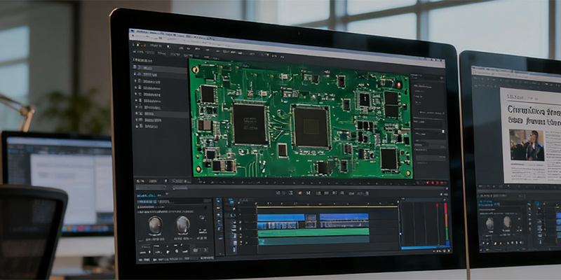
Highprecision scanning and accurate data extraction are the core foundational processes of all PCB copy and cloning services, determining the fidelity, manufacturability, and functional consistency of replicated circuit boards. Many physical PCB samples provided by customers have no original design files, incomplete technical documents, blurred circuit traces, or damaged local structures, making manual drawing and data sorting prone to errors, omissions, and deviation. Professional PCB copy board scanning and data extraction services adopt a fullprocess automated and semiautomated precision detection system, breaking through the limitations of manual operation, and realizing comprehensive, accurate, and digitized restoration of PCB physical structure, circuit distribution, and component layout data. This standardized data acquisition process lays a solid foundation for subsequent schematic reconstruction, BOM sorting, PCB layout restoration, and mass production.
The scanning process covers fulldimensional detection of singlelayer, doublelayer, and multilayer PCBs, including surface circuit scanning, internal buried and blind hole detection, copper layer thickness measurement, solder mask and silk screen scanning, and mechanical outline precision positioning. For ordinary single and doublelayer boards, we use highdefinition industrial optical scanners to capture micronlevel circuit trace width, spacing, and pad position data, with a scanning accuracy up to 0.01mm. For complex multilayer boards with hidden internal circuits that cannot be observed optically, we cooperate with nondestructive Xray scanning equipment to layerbylayer identify internal copper foil circuits, via connections, and insulating layer structures, avoiding board disassembly and damage to customer samples. All scanning data is automatically stored and sorted into standardized digital files to ensure no data loss or distortion during transmission and sorting.
Data extraction is a refined sorting and verification process based on scanning raw data, including circuit network data extraction, component position coordinate extraction, mechanical size parameter extraction, and electrical connection logic sorting. Our engineers will eliminate scanning noise, correct tiny deviation data, and verify the electrical connectivity of each circuit node one by one to ensure that the extracted data is completely consistent with the physical board. After preliminary data extraction, we will conduct secondary simulation verification and physical comparison calibration to eliminate open circuits, short circuits, and connection errors caused by scanning errors. The final output complete data package includes PCB outline parameters, layer stack parameters, circuit network tables, component coordinate files, and hole position parameter files, which can be directly used for subsequent design editing, proofing production, and technical archiving. This onestop scanning and data extraction service greatly improves the efficiency and accuracy of PCB copying, shortens the project cycle, and avoids rework losses caused by inaccurate basic data.

Email: 15361682656@163.com
Factory: Room 703, Kelunte R&D Building, No. 1 Ganli 5th Road, Jihua Street, Longgang District, Shenzhen City