CN
-
Service Hotline
15766086363


Release Date:Aug 11, 2026
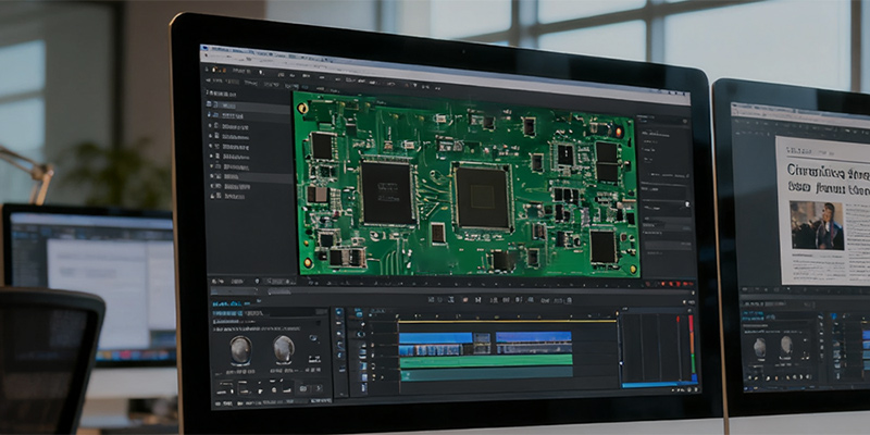
Micro blind hole PCB reverse cloning is a high-precision electronic reverse engineering technology dedicated to copying printed circuit boards with micro-scale blind hole structures, which is widely applied in high-end consumer electronics, wearable devices, 5G communication modules and miniature industrial control equipment. Different from conventional through-hole PCB cloning, the core difficulty of micro blind hole PCB cloning lies in the ultra-small aperture size, layered conduction characteristics and hidden structural design of blind holes. The micro blind holes involved in this process usually have an aperture of less than 0.15mm, and the hole depth ratio is strictly controlled within the industrial standard, realizing layered electrical connection between the surface layer and the inner layer of the PCB without penetrating the entire board, which effectively saves board space and improves circuit integration.
The reverse cloning process of micro blind hole PCB adopts a standardized and high-precision technical workflow. Firstly, professional non-destructive testing equipment such as X-ray fluorescence detector and industrial high-definition microscope is used to scan and analyze the original board. This step aims to accurately capture the position, aperture, depth, layered connection relationship and copper thickness of all micro blind holes, avoiding structural damage to the original sample board. Conventional mechanical disassembly is abandoned in this link to prevent micro hole deformation and inner circuit breakage caused by external force. After completing the structural scanning, engineers will carry out layered data sorting, distinguish blind holes, buried holes and through-holes one by one, and mark the electrical network attribution of each micro blind hole to ensure that the interlayer conduction logic is completely consistent with the original board.
In the circuit data reverse derivation stage, high-precision PCB scanning software is used to restore the original board’s wiring diagram, component distribution diagram, solder mask diagram and silk screen layer diagram. For micro blind hole areas with tiny structures, manual secondary calibration is required to correct the deviation of automatic scanning data, especially for dense blind hole arrays in high-precision areas such as chip pins and radio frequency circuits. After the completion of data restoration, the engineer will conduct DFM (Design for Manufacturability) inspection on the derived PCB file, optimize the micro blind hole process parameters, adjust the laser drilling aperture tolerance and electroplating copper thickness parameters, and eliminate manufacturing risks such as hole wall copper leakage and blind hole open circuit in advance.
The manufacturing and verification stage is the key to ensure the yield of micro blind hole PCB cloning. In the production process, laser drilling technology is adopted instead of traditional mechanical drilling to ensure the dimensional accuracy of micro blind holes. The electroplating process strictly controls the current density and plating time to ensure uniform copper deposition on the hole wall and meet the interlayer conduction resistance standard. After the production of the cloned board is completed, multi-dimensional testing is carried out, including X-ray hole structure detection, interlayer conduction resistance testing, high and low temperature cycling reliability testing and impedance testing of blind hole circuits. Only when all parameters are consistent with the original board can the cloned product be delivered. With the continuous miniaturization of electronic equipment, micro blind hole PCB reverse cloning has become an indispensable technical means in the field of PCB imitation and secondary development, providing efficient and reliable technical support for enterprise product upgrading and alternative research and development.

Email: 15361682656@163.com
Factory: Room 703, Kelunte R&D Building, No. 1 Ganli 5th Road, Jihua Street, Longgang District, Shenzhen City