CN
-
Service Hotline
15766086363


Release Date:Mar 25, 2026
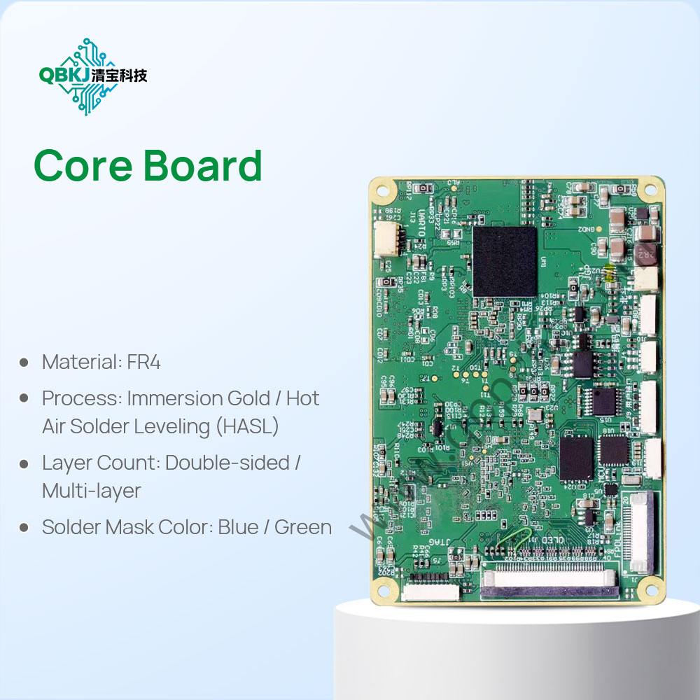
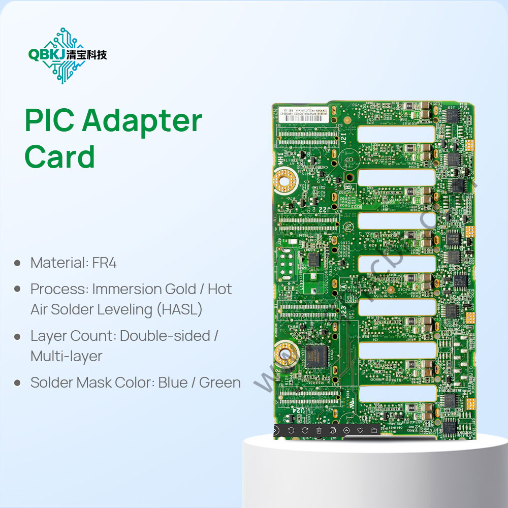
With the rapid development of electronic technology, electronic devices are becoming increasingly miniaturized, high-performance, and multi-functional, which puts higher requirements on PCB (Printed Circuit Board) and PCBA (Printed Circuit Board Assembly). High-precision multilayer PCB PCBA, with its advantages of high density, small size, stable signal transmission, and high space utilization, has become the core component of high-end electronic products in fields such as 5G communication, medical equipment, industrial control, and aerospace. High-precision multilayer PCB PCBA processing involves a series of complex and sophisticated processes, requiring strict control of each link to ensure the accuracy, reliability, and performance of the final product.
The processing of high-precision multilayer PCB PCBA starts with raw material selection and parameter confirmation, which is the foundation of product quality. In terms of substrate selection, high-Tg FR4, Rogers, or other high-performance materials are preferred, which have good thermal stability, mechanical strength, and electrical performance, ensuring that the PCB can maintain stable performance under high temperature, high humidity, and other harsh conditions. The copper foil used must have uniform thickness, low surface roughness, and good conductivity, to avoid problems such as uneven plating and poor solder joint adhesion during subsequent processing. The semi-cured sheet, which is used to bond multiple layers of substrates, must have stable resin content and fluidity, ensuring good bonding effect and overall flatness of the multilayer PCB.
Before formal processing, detailed design review and stack-up planning are required. Engineers conduct in-depth DFM (Design for Manufacturability) analysis to check the rationality of the circuit design, including the layout of components, the width and spacing of lines, the position and size of holes, and the design of the ground plane, to avoid design flaws that may affect processing and performance. Stack-up planning is particularly important for multilayer PCBs, as it directly affects the signal integrity, electromagnetic compatibility, and mechanical strength of the product. Engineers need to reasonably arrange the number of layers, the thickness of each layer, the distribution of copper foil, and the position of blind/buried vias, ensuring symmetry in copper distribution and layer arrangement to prevent the PCB from warping or twisting during processing and use.
The core processing steps of high-precision multilayer PCB include inner layer processing, lamination, drilling, plating, and surface treatment. In inner layer processing, the circuit pattern is transferred to the inner substrate through processes such as cleaning, micro-roughening, and exposure and development, with strict control of pattern accuracy to ensure that the line width and spacing meet the design requirements (minimum line width and spacing can reach 2mil/2mil). After inner layer processing, the inner substrate is inspected using AOI equipment to detect defects such as open circuits, short circuits, and pattern deviations, ensuring the quality of the inner layer.
Lamination is the key step to form a multilayer PCB, which involves stacking the inner substrates, semi-cured sheets, and outer substrates in a certain order, and bonding them into a single body through high temperature and high pressure. During lamination, strict control of temperature, pressure, and time is required to ensure that the semi-cured sheet melts and flows evenly, filling the gaps between the layers and forming a firm bond. The lamination process must ensure that the layers are aligned accurately, with layer alignment deviation controlled within a very small range (usually within ±0.02mm), to avoid affecting the interlayer connection and signal transmission. After lamination, the multilayer PCB is subjected to processes such as deburring and cleaning to remove burrs and impurities on the surface and edges.
Drilling is used to realize interlayer connection, with high requirements for hole position accuracy, hole size accuracy, and hole wall quality. High-precision drilling equipment, such as CNC drilling machines and laser drilling machines, is used, with CCD visual positioning system to real-time correct the drilling position, ensuring that the hole position deviation is within the design range. For micro盲孔 and buried vias, laser drilling technology is adopted, which has high drilling accuracy and can process very small holes (minimum hole size up to 0.1mm). After drilling, the hole wall is treated through processes such as desmearing and chemical copper plating to ensure good conductivity of the hole wall. Electroplating copper is then performed to thicken the copper layer on the hole wall and the surface of the PCB, meeting the conductive performance requirements.
Surface treatment is used to improve the solderability, corrosion resistance, and wear resistance of the PCB surface, with common methods including immersion gold (ENIG), spray tin (HASL), and OSP (Organic Solderability Preservative). For high-precision multilayer PCBA, immersion gold is often preferred, as it has good conductivity, flatness, and corrosion resistance, ensuring the quality of solder joints and the stability of signal transmission. After surface treatment, the PCB is inspected again to ensure that there are no defects such as missing plating, uneven plating, or scratches.
The final step is PCBA assembly and testing. High-precision SMT assembly lines are used to assemble components such as BGA, QFN, and 01005 small-sized components, with high placement accuracy to ensure the reliability of the assembly. Soldering is performed using lead-free soldering technology, with strict control of soldering parameters to avoid defects such as cold solder, bridging, and solder balls. After assembly, multiple tests are conducted, including AOI inspection, X-ray inspection, ICT testing, functional testing, and aging testing, to ensure that the PCBA meets the design requirements and performance indicators. High-precision multilayer PCB PCBA processing requires professional technical capabilities, advanced production equipment, and strict quality control systems, which can provide high-quality core components for high-end electronic products, promoting the development of the electronic industry.
Email: 1330695973@qq.com
Factory: Room 703, Kelunte R&D Building, No. 1 Ganli 5th Road, Jihua Street, Longgang District, Shenzhen City