CN
-
Service Hotline
15766086363


Release Date:Mar 03, 2026
Hardware Design Reverse (also called Hardware Reverse Engineering) is a broad process that extracts the design logic, architecture, and specifications of physical electronic hardware—encompassing PCBs, PCBAs, and larger systems (e.g., IoT devices, industrial controllers)—to understand how the hardware functions, interacts with software, or can be modified. Unlike PCB-focused reverse engineering, this process includes analyzing mechanical components (e.g., enclosures, connectors) and software-hardware integration (e.g., firmware-IC communication).
The workflow begins with System-Level Analysis: Technicians document the hardware’s overall function (e.g., a smart thermostat’s temperature sensing and connectivity features) and identify key subsystems (e.g., power management, wireless module, microcontroller). Mechanical components are measured or 3D-scanned to replicate enclosures or mounting interfaces.
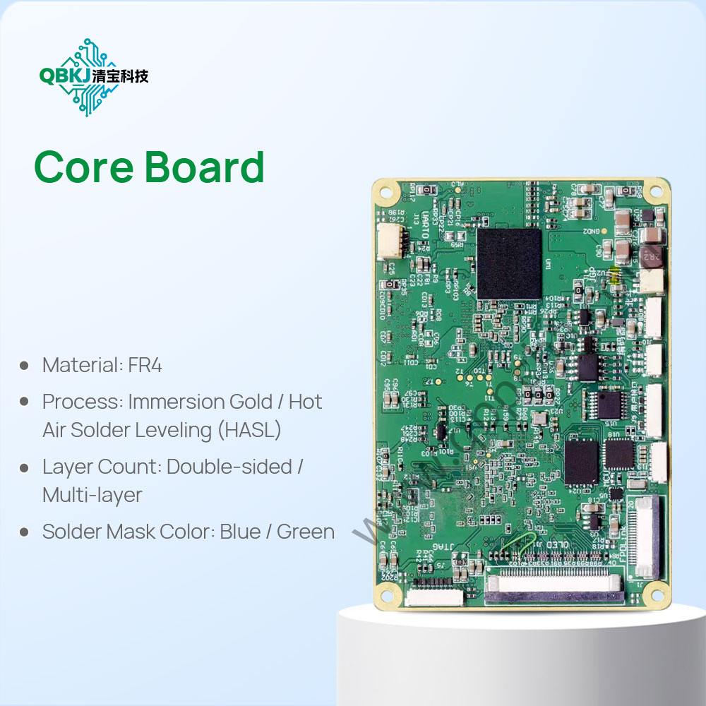
Next is Component-Level Reverse Engineering: For PCBs/PCBAs within the hardware, the process follows standard PCBA reverse steps (teardown, component analysis, trace mapping) to generate schematics and BOMs. For non-PCB components (e.g., sensors, motors), datasheets are sourced to document specifications (e.g., sensor accuracy, motor torque).
Then comes Software-Hardware Interface Mapping: Using tools like logic analyzers or JTAG debuggers, experts trace how firmware communicates with hardware components—e.g., how a microcontroller sends commands to a display module. This includes decoding communication protocols (I2C, SPI) and identifying firmware storage locations (e.g., EEPROM, flash memory).
Finally, Design Reconstruction & Validation: The extracted data is compiled into a complete hardware design package, including mechanical CAD files, PCB schematics, BOMs, and interface protocols. A prototype of the reversed hardware is built and tested to ensure it matches the original’s functionality—including software compatibility. This process is vital for legacy hardware maintenance, product upgrades (e.g., adding IoT connectivity to older devices), and competitive analysis. Challenges include decoding proprietary firmware (requiring advanced debugging skills) and replicating custom ASICs (application-specific integrated circuits), which often lack public datasheets.
Email: 1330695973@qq.com
Factory: Room 703, Kelunte R&D Building, No. 1 Ganli 5th Road, Jihua Street, Longgang District, Shenzhen City