CN
-
Service Hotline
15766086363


Release Date:Apr 02, 2026
Double-sided multi-layer PCBA SMT (Surface Mount Technology) processing is a core service in the electronics manufacturing industry, designed to meet the growing demand for miniaturization, high density, and high performance of electronic products. With the rapid development of consumer electronics, industrial control, automotive electronics, and aerospace fields, traditional single-sided or simple double-sided PCBA can no longer satisfy the functional requirements of complex electronic systems. Double-sided multi-layer PCBA, by integrating multiple layers of circuits on both sides of the substrate, not only effectively reduces the size and weight of the circuit board but also improves the signal integrity, reduces electromagnetic interference, and enhances the overall reliability of the electronic product.
The processing process of double-sided multi-layer PCBA SMT is highly complex and requires strict control of each link to ensure product quality. The entire process starts with substrate selection, where high-quality FR-4, high-frequency materials, or other special substrates are chosen according to the product’s application scenario and performance requirements. The substrate must have excellent thermal conductivity, insulation performance, and mechanical strength to withstand the high-temperature environment during soldering and the long-term operation of the product. Next, the substrate undergoes processes such as cutting, drilling, and copper plating. Drilling is a key link, as the precision of the holes directly affects the connection between layers and the mounting of components. With the help of advanced CNC drilling machines, we can achieve hole diameters as small as 0.1mm, ensuring the accuracy and consistency of each hole.
After the substrate processing is completed, the SMT mounting process begins. First, solder paste printing is performed on both sides of the substrate. The solder paste is evenly applied to the pad positions through a stencil, and the thickness and uniformity of the solder paste are strictly controlled to avoid problems such as cold soldering or bridging. Then, surface mount components (SMDs) of various sizes and types, including resistors, capacitors, integrated circuits (ICs), diodes, and transistors, are accurately placed on the solder paste by high-speed SMT placement machines. These placement machines are equipped with high-precision vision systems that can identify the position of the pads and the components, ensuring that each component is placed correctly with a placement accuracy of up to ±0.03mm.
After component placement, the substrate enters the reflow soldering oven. The reflow soldering process is carried out in a controlled temperature environment, with different temperature zones (preheating zone, soaking zone, reflow zone, and cooling zone) set to ensure that the solder paste melts completely, wets the pads and component pins, and forms a firm solder joint after cooling. For double-sided PCBA, the soldering process needs to be performed twice—first soldering one side, then flipping the board to solder the other side. During the second soldering, special fixtures are used to protect the components that have already been soldered to avoid damage or displacement.
In addition to the basic SMT processing steps, double-sided multi-layer PCBA also requires processes such as layer pressing, via hole filling, and surface treatment. Layer pressing is to bond multiple layers of circuit boards together through high temperature and high pressure, ensuring the stability and reliability of the interlayer connection. Via hole filling is to fill the through holes with conductive materials to enhance the electrical conductivity and mechanical strength of the holes. Surface treatment methods such as HASL (Hot Air Solder Leveling), ENIG (Electroless Nickel Immersion Gold), and OSP (Organic Solderability Preservative) are adopted to improve the solderability of the pads, prevent oxidation, and extend the service life of the PCBA.
Quality control is an integral part of double-sided multi-layer PCBA SMT processing. We have established a comprehensive quality inspection system, including incoming inspection (for substrates, components, solder paste, etc.), in-process inspection (such as solder paste printing inspection, component placement inspection, and reflow soldering inspection), and final inspection (such as visual inspection, X-ray inspection, and functional testing). X-ray inspection is particularly important for multi-layer PCBA, as it can detect internal defects such as voids, cold soldering, and misalignment of interlayer connections that cannot be observed by the naked eye. Functional testing is carried out according to the customer’s requirements to ensure that the PCBA can work normally under the specified conditions.
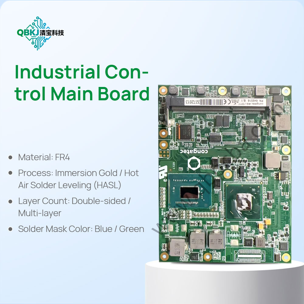
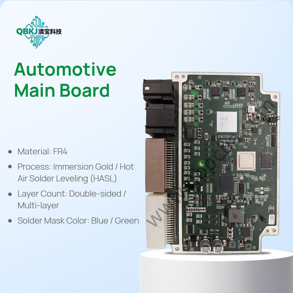
The application scope of double-sided multi-layer PCBA SMT processing is extremely wide. In the consumer electronics field, it is used in smartphones, tablets, laptops, smart wearables, and other products, where miniaturization and high performance are required. In the industrial control field, it is applied to industrial controllers, sensors, and automation equipment, requiring high reliability and stability. In the automotive electronics field, it is used in on-board infotainment systems, engine control units (ECUs), and advanced driver assistance systems (ADAS), which need to withstand harsh environmental conditions such as high temperature, vibration, and humidity. In the aerospace field, it is used in aircraft navigation systems, satellite communication equipment, and other high-precision products, requiring extremely high quality and reliability.
As a professional double-sided multi-layer PCBA SMT processing manufacturer, we have advanced production equipment, a professional technical team, and a strict quality management system. We can provide customized processing services according to the customer’s specific requirements, including substrate selection, circuit design optimization, component procurement, SMT mounting, soldering, testing, and packaging. Our goal is to provide customers with high-quality, high-reliability PCBA products, helping customers reduce production costs, shorten delivery cycles, and enhance their market competitiveness. Whether it is small-batch prototype production or large-batch mass production, we can meet the diverse needs of customers with efficient and professional services.
Email: 1330695973@qq.com
Factory: Room 703, Kelunte R&D Building, No. 1 Ganli 5th Road, Jihua Street, Longgang District, Shenzhen City