CN
-
Service Hotline
15766086363


Release Date:Mar 05, 2026
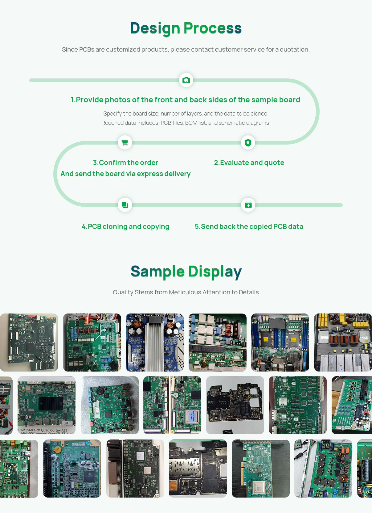
Reverse PCBA Layout extends reverse PCB layout by integrating the physical placement and orientation of components on a Printed Circuit Board Assembly (PCBA) — going beyond the bare PCB’s structure to include how active/passive components (e.g., ICs, resistors, capacitors) are mounted and aligned on the board. Unlike reverse PCB layout (which focuses on the unpopulated board), PCBA layout reverse engineering ensures that any duplicated or modified PCBA retains the original’s component compatibility, thermal management, and mechanical fit (e.g., with enclosures or connectors).
The process begins with PCBA Documentation: The assembled board is scanned using a 3D optical scanner to capture component positions (X/Y/Z coordinates) and orientations (e.g., diode polarity, IC pin 1 alignment). High-resolution images of the top and bottom sides are taken to document component labels (part numbers, values) and solder joint profiles.
Next is Component Footprint Cross-Referencing: Each component’s package type (e.g., 0402 SMD, DIP-14, QFP-64) is identified via datasheets, and its footprint is matched to the reversed PCB layout (from reverse PCB layout process). This ensures that the component’s pads align with the PCB’s pads exactly — a critical step for avoiding assembly errors.
Then comes Layout Integration: The component placement data is overlaid onto the reversed PCB layout file. Technicians adjust component positions to match the 3D scan data, ensuring that clearances (between components, between components and board edges) meet the original’s specifications — this is vital for thermal performance (e.g., avoiding overheating from closely packed power components) and mechanical fit (e.g., ensuring connectors align with enclosure ports).
Finally, Validation: A prototype PCBA is assembled using the reversed layout and validated via visual inspection (checking component alignment) and functional testing (confirming no electrical issues from misplacement). AOI (Automated Optical Inspection) is used to compare the prototype to the original PCBA’s 3D scan. Challenges include replicating manual component placements (e.g., odd-form connectors) and ensuring that thermal vias under heat-generating components are correctly positioned. This process is critical for repairing legacy PCBAs or customizing assemblies for new components.
Email: 1330695973@qq.com
Factory: Room 703, Kelunte R&D Building, No. 1 Ganli 5th Road, Jihua Street, Longgang District, Shenzhen City