CN
-
Service Hotline
15766086363


Release Date:Dec 16, 2025
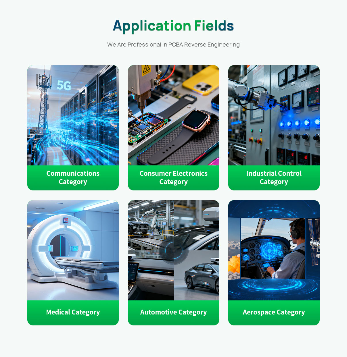
The PCBA Copy Process is a structured, step-by-step workflow that transforms an original PCBA into one or more functional cloned units—ensuring accuracy, consistency, and reliability. This standardized process minimizes errors, streamlines production, and provides clarity for businesses, making it applicable across industries (e.g., consumer electronics, industrial control, medical devices) and PCB types (e.g., 2-layer, multi-layer, high-density).
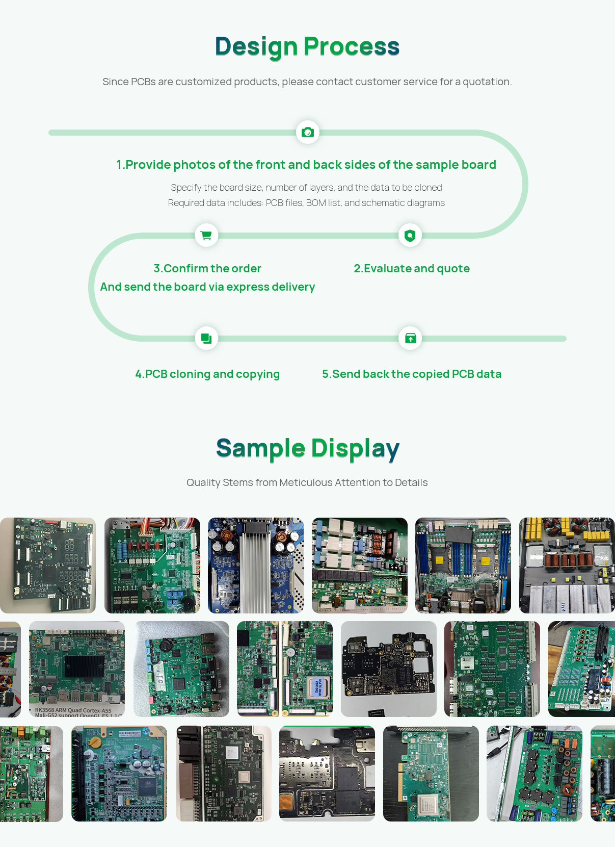
Step 1: Pre-Copy Preparation and Assessment
The process starts with evaluating the original PCBA: engineers confirm the board is functional (non-functional PCBs require additional repair steps), document basic attributes (size, layer count, component types), and assess copy feasibility (e.g., identifying encrypted firmware or custom ICs that may require specialized handling). They also review client requirements (e.g., production volume, timeline, compliance standards like RoHS) to tailor the process—for example, high-volume orders will prioritize manufacturability steps, while legacy PCB copies focus on obsolete component sourcing.
Step 2: Physical Data Capture
Engineers use specialized tools to capture every detail of the original PCBA:
Optical Scanning: High-resolution scanners (1–5 micron resolution) capture top/bottom layers, silkscreen markings, and component placement—creating digital images for reference.
X-ray Imaging: For multi-layer PCBs or components with hidden connections (e.g., BGAs), X-rays map internal layers, via positions, and solder ball connections.
Component Documentation: Each component is identified via visual inspection (part numbers, value codes) or testing (for unmarked parts like resistors/capacitors). Engineers record part numbers, manufacturers, package types, and specifications in a preliminary BOM.
Step 3: Reverse Engineering to Digital Design
The captured data is converted to digital design files using PCB design software (e.g., Altium Designer, KiCad):
Schematic Reconstruction: Engineers trace signal paths (using multimeter checks for connectivity) to create a circuit schematic—documenting how components interact.
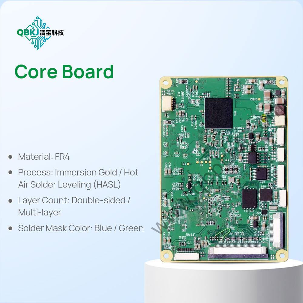
PCB Layout Recreation: The layout is recreated to match the original’s trace routing, via sizes, layer stack-up, and component positions. Impedance-controlled traces (for high-speed PCBs) and thermal management features (e.g., copper pours) are replicated with precision.
BOM Finalization: The preliminary BOM is validated and expanded to include sourcing information (distributors, lead times) and compliance data.
Step 4: Prototype Fabrication and Testing
A prototype cloned PCBA is fabricated and tested to validate the design:
Prototype Production: The digital design is used to manufacture a small-batch prototype (1–5 units), with components sourced to match the original.
Validation Testing: Prototypes undergo electrical tests (continuity, voltage/current checks), functional tests (to confirm they match the original’s performance), and visual inspection (AOI for solder defects). Any discrepancies (e.g., signal delays, component misbehavior) trigger design revisions and re-prototyping.
Step 5: Production (Optional)
For clients needing multiple units, the validated design moves to production:
Bulk Fabrication: PCBs are manufactured in volume, with automated processes (etching, drilling) ensuring consistency.
Component Assembly: SMT pick-and-place machines populate PCBs, followed by wave soldering (for THT components) and AOI inspection.
Final Testing: Each production unit undergoes functional and electrical testing to ensure quality.
Key benefits of a standardized process include consistency: every cloned PCBA meets the same quality standards. It also ensures transparency: clients can track progress at each step, reducing uncertainty. When selecting a provider, prioritize those with a documented, repeatable process and quality control checkpoints at each stage (e.g., after reverse engineering, prototype testing) to avoid errors.
Email: 1330695973@qq.com
Factory: Room 703, Kelunte R&D Building, No. 1 Ganli 5th Road, Jihua Street, Longgang District, Shenzhen City