CN
-
Service Hotline
15766086363


Release Date:Aug 14, 2026
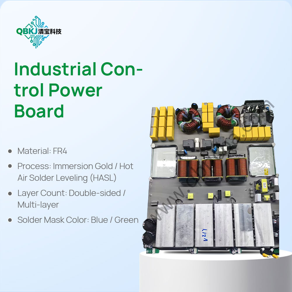
Thick copper PCB clone is a professional reverse cloning technology for high-current, high-power printed circuit boards with copper thickness greater than 3oz (105μm), which is widely used in power supply equipment, inverter modules, new energy power control systems, industrial high-current distribution equipment and automotive power electronic systems. Ordinary PCBs usually use 1oz or 2oz copper foil, while thick copper PCBs adopt 3oz-10oz thick copper materials, which have ultra-high current carrying capacity, strong over-current impact resistance and good heat dissipation performance. Thick copper PCB clone focuses on restoring the thick copper circuit structure, over-current performance and process characteristics of the original board, realizing the accurate replication of high-power circuit boards.
The technical difficulties of thick copper PCB clone are concentrated in thick copper circuit scanning and data restoration, thick copper etching process matching and over-current performance replication. Due to the thick copper layer of the original board, the traditional scanning method is prone to errors in circuit depth and line side wall structure detection. Therefore, the cloning process adopts industrial 3D microscopic scanning technology to accurately collect the line width, line thickness, side wall roughness and copper thickness of each circuit of the original thick copper PCB, and record the layout of high-current circuits, heat dissipation copper blocks and thick copper bonding pads. At the same time, the board thickness, substrate material, insulation layer parameters and via copper thickness of the original board are detected to form a complete original board parameter database.
In the data sorting and file optimization stage of thick copper PCB clone, engineers classify high-current circuits and low-current signal circuits separately, accurately restore the thick copper wiring path and node connection relationship, and ensure that the over-current cross-sectional area of each power circuit is completely consistent with the original board. For the thick copper lap joint and hole copper plating areas of the original board, the process parameters are calibrated in detail to avoid over-current heating and circuit burnout caused by insufficient lap joint area and thin hole copper. In addition, combined with the high-power operation characteristics of thick copper PCB, the insulation spacing between circuits is optimized to meet the high-voltage insulation safety standards of power equipment.
The manufacturing process of thick copper PCB clone is far more complex than ordinary PCB production. In the etching process of thick copper circuits, secondary precision etching technology is adopted to ensure smooth circuit side walls, no burrs and short circuits, and accurate line size. In the electroplating process of through holes and blind holes, prolonged thick copper electroplating is carried out to ensure that the hole wall copper thickness meets the high-current conduction requirements. The lamination process uses high-temperature and high-pressure resistant prepreg materials to avoid delamination and bulging of the board caused by high-temperature heating during high-power operation. At the same time, the solder mask ink with high temperature resistance and high insulation performance is selected to adapt to the high-temperature working environment of thick copper PCB.
The finished product testing of thick copper PCB clone focuses on over-current performance and reliability testing. Including ultra-high current load test, long-term power-on aging test, circuit temperature rise test, insulation resistance test and mechanical strength test. It is necessary to verify that the cloned thick copper PCB can work stably for a long time under rated high current, without overheating, voltage drop and circuit damage. Thick copper PCB clone solves the technical pain points of difficult design and high research and development cost of high-power thick copper circuit boards, helps new energy and power electronic enterprises quickly realize product imitation and batch production, and provides solid technical support for the localization and upgrading of high-power electronic equipment.

Email: 15361682656@163.com
Factory: Room 703, Kelunte R&D Building, No. 1 Ganli 5th Road, Jihua Street, Longgang District, Shenzhen City