CN
-
Service Hotline
15766086363


Release Date:Nov 06, 2026
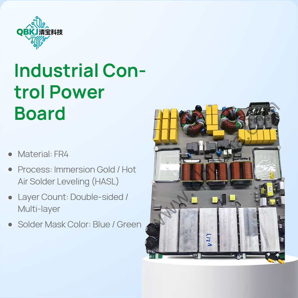
An inverter PCB clone power circuit copy service is focused on the authorized reverse engineering and reproduction of inverter boards used in motor drives, solar inverters, uninterruptible power supplies, induction heating, and variablefrequency drives. Inverter PCBs contain a control section, a power stage, gate drivers, current and voltage sensing, protection circuits, and communication interfaces. The power circuit is the most critical part because it converts DC to AC using highspeed switching devices such as IGBTs, MOSFETs, or SiC transistors. When original design files are unavailable, a professional clone service can recreate the board by extracting the schematic, analyzing the power topology, and generating new manufacturing data. The goal is to produce a reliable replacement that matches the original electrical and thermal performance while respecting all intellectual property rights.
The inverter PCB reverseengineering process begins with a detailed inspection of the power stage and control stage. Engineers identify the DC bus, bulk capacitors, snubber circuits, gate drive transformers or optocouplers, current sensors, shunt resistors, and heat sinks. Highresolution imaging and layer delayering may be used to recover copper traces and ground planes. The team then extracts the netlist, creates a schematic, and builds a bill of materials. Critical components such as IGBT modules, gate driver ICs, DSPs, microcontrollers, and Hall sensors are documented. The PCB layout is recreated with attention to highcurrent paths, creepage, clearance, thermal relief, and electromagnetic compatibility. Prototypes are fabricated, assembled, and tested with resistive, inductive, and motor loads. The final deliverables usually include schematics, PCB files, Gerber data, assembly drawings, and a test report.
Inverter power circuits are technically challenging because they combine high voltage, high current, and highfrequency switching. Parasitic inductance in the DC bus and gate loops can cause voltage spikes, ringing, and device failure. Gate drive timing must be precise to prevent shootthrough. Dead time, desaturation protection, overcurrent protection, and thermal shutdown must function correctly. Current sensing must be accurate for torque control and fault detection. Cooling design affects reliability, especially in enclosed industrial environments. EMI is a major concern because fast switching generates conducted and radiated noise. The control section must handle realtime PWM generation, encoder feedback, and communication protocols such as CAN, Modbus, or EtherCAT. If firmware is proprietary, the customer must provide legal authorization or legally obtained firmware. A successful inverter PCB clone must therefore be more than a visual copy; it must be a validated power electronics design.
Testing and compliance are essential for any inverter PCB clone power circuit copy project. The board should be tested at low voltage first, then gradually brought up to full power with currentlimited supplies. Engineers measure switching waveforms, efficiency, thermal rise, fault response, and EMI. Functional tests may include motor spin, torque control, acceleration, braking, and fault injection. Safety standards such as IEC 61800, UL 508C, and applicable grid codes may apply depending on the application. Documentation must clearly state that the service is for authorized reverse engineering and that the customer is responsible for final certification. Unauthorized copying of branded inverter designs is prohibited. When performed professionally, inverter PCB cloning can help repair obsolete drives, support legacy industrial equipment, and provide reliable replacement power boards for critical applications.

Email: 15361682656@163.com
Factory: Room 703, Kelunte R&D Building, No. 1 Ganli 5th Road, Jihua Street, Longgang District, Shenzhen City