CN
-
Service Hotline
15766086363


Release Date:Nov 09, 2026
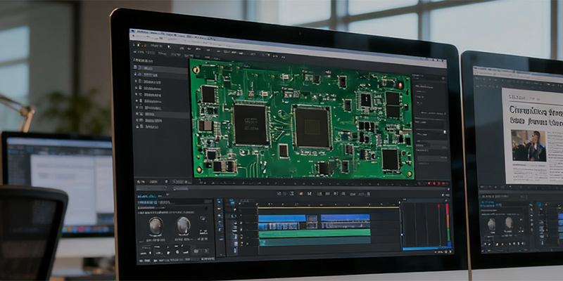
HDI PCB copy microvia board cloning is a highend precision reverse engineering service for HDI (High Density Interconnect) circuit boards with microvia structures. HDI boards adopt microvia technology, ultrafine traces, and ultrasmall pad design, which have the characteristics of high circuit density, small size, light weight, and excellent signal transmission performance. They are core circuit boards of highend precision electronic products such as smart phones, tablet computers, wearable devices, 5G communication modules, and precision medical electronics. Microvias are tiny conductive holes with ultrasmall aperture, which realize interlayer connection of highdensity circuits, making HDI board cloning one of the most technically difficult PCB duplication services in the industry.
Our HDI PCB microvia board cloning service adopts international leading highprecision detection and reverse engineering technology to break through the technical bottleneck of microstructure duplication. The microvias of HDI boards have extremely small apertures, usually only 0.050.15mm, with dense distribution and multilayer staggered conduction structures, which cannot be identified by ordinary detection equipment. We use ultrahigh resolution industrial microscopes and 3D tomography scanning equipment to conduct fullangle and fulllayer detection of the original HDI board, accurately collecting microvia aperture, hole depth, hole spacing, layered conduction relationship, ultrafine trace width, and pad spacing parameters, realizing fulldata restoration of microscale circuit structures.
In the design file restoration and optimization stage, our senior PCB engineers sort out the highdensity circuit logic and microvia conduction rules layer by layer, restore standard HDI design files, complete schematic diagrams, and accurate BOM lists. For the stacked microvia and buried via composite structures of highend HDI boards, we accurately restore the stacked position and conduction sequence of each microvia, and optimize the microvia layout and trace routing according to highspeed signal transmission standards, effectively avoiding signal crosstalk, impedance mismatch, and transmission delay problems in highdensity circuits. All design parameters strictly comply with international HDI board manufacturing specifications to ensure the consistency of circuit performance and structural precision.
The production and testing of cloned HDI microvia boards adopt ultraprecision manufacturing processes and strict quality inspection standards. We use laser microdrilling technology to process microvias, ensuring the precision of hole position and aperture, and adopt professional electroplating technology to ensure uniform and dense copper plating on the hole wall and stable conduction performance. Finished HDI boards will undergo professional highspeed signal testing, impedance testing, microvia conduction fatigue testing, and high and low temperature reliability testing to verify the stability of microvia structure and highdensity circuits under longterm highspeed operation. Our HDI microvia board cloning service supports firstorder, secondorder and multiorder HDI board duplication, providing accurate and reliable circuit duplication solutions for highend miniaturized and highdensity electronic products.

Email: 15361682656@163.com
Factory: Room 703, Kelunte R&D Building, No. 1 Ganli 5th Road, Jihua Street, Longgang District, Shenzhen City