CN
-
Service Hotline
15766086363


Release Date:Aug 10, 2026
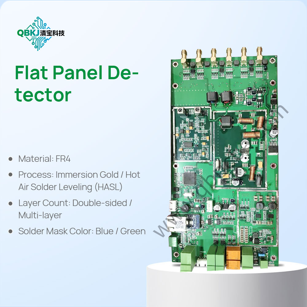
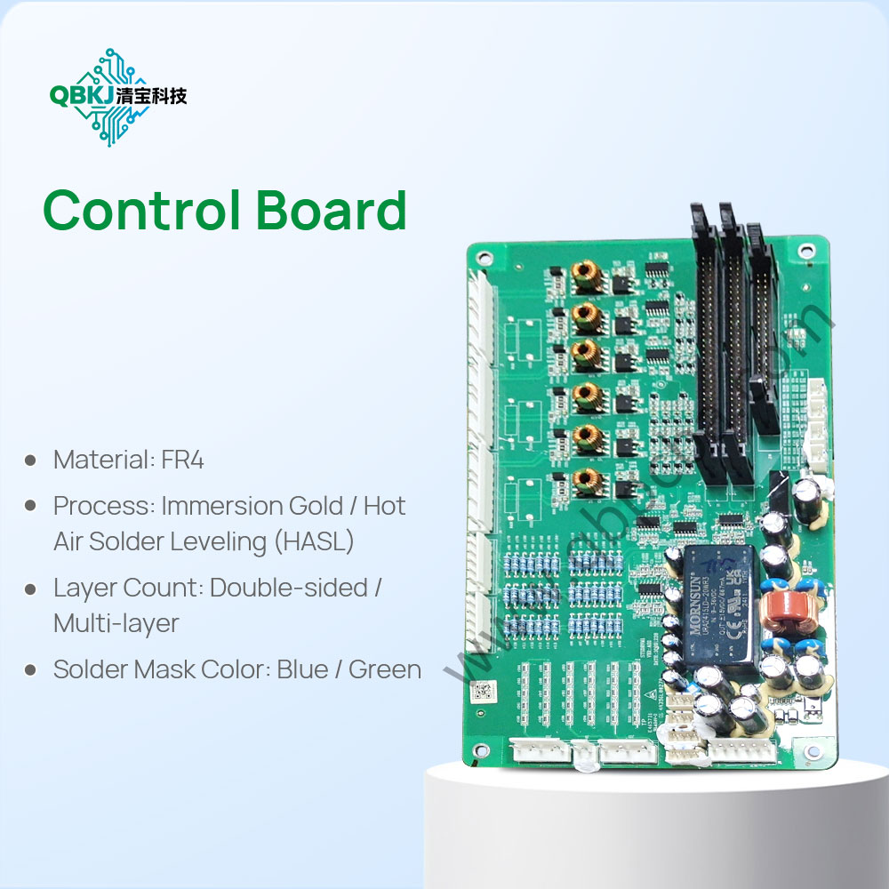
2-layer PCB clone, namely double-sided printed circuit board cloning, is the most basic, mature and widely used service type in PCB reverse engineering and replication industry. A 2-layer PCB consists of two conductive copper layers (top layer and bottom layer) and intermediate insulating dielectric layers, with circuit wiring on both the front and back sides of the board, and the upper and lower circuits are connected through metal via holes. Due to its simple structure, low production cost, short processing cycle and stable performance, 2-layer PCBs are widely used in various ordinary electronic equipment, consumer electronic products, small industrial control equipment, power supply modules and household appliances, making 2-layer PCB clone the most demanded basic service in the electronic manufacturing supporting industry.
Our 2-layer PCB clone service adopts a full-process non-destructive high-precision replication process, which can completely restore all design parameters and functional performance of the original double-sided circuit board. The whole service process is standardized and refined, including original board detection, high-precision scanning, circuit analysis, schematic restoration, PCB layout redrawing, BOM sorting, prototype proofing and functional testing. For the structural characteristics of 2-layer PCBs with no inner layer circuit and simple wiring logic, we optimize the cloning process, greatly shorten the reverse cycle, and realize fast and high-precision replication on the premise of ensuring 100% consistency.
In the parameter detection and scanning stage, we use high-resolution industrial microscopes and 3D scanning equipment to fully collect the line width, line spacing, via hole diameter, pad size, board thickness, substrate material and surface treatment process of the original 2-layer PCB. Different from multi-layer boards, 2-layer PCBs have all circuits exposed on the front and back sides, so we can realize full-data non-destructive collection without splitting the board, completely protecting the integrity of the customer's original sample board. Through professional reverse engineering software, we automatically identify and manually verify the circuit connection logic of the upper and lower layers one by one, eliminate wiring errors and short circuit risks, and ensure that the restored circuit diagram and PCB layout are completely consistent with the original board.
In the production and proofing stage of 2-layer PCB clone, we strictly select high-quality FR-4 substrate materials, electrolytic copper foil and environmental protection solder mask ink matching the original board, and adopt standardized double-sided board production process. The via hole metallization process, solder mask printing process, silk screen character printing process and surface treatment processes (including tin spraying, gold plating, silver plating and OSP anti-oxidation) are all restored in accordance with the original board standards. The produced cloned 2-layer PCB has flat board surface, clear lines, accurate hole positions, stable conductivity and good insulation performance, with all physical and electrical parameters meeting international IPC manufacturing standards.
2-layer PCB clone has a wide range of application scenarios and powerful practical value. In the consumer electronics industry, it is applicable to the cloning and production of small electronic products such as power banks, Bluetooth speakers, remote controls, charging heads and small smart sensors. In the industrial field, it is used for the replication of ordinary industrial control circuit boards, relay control boards, switching power supply boards and equipment drive boards. In the field of household appliances, it is widely used in the cloning of circuit boards of televisions, air conditioners, washing machines, electric fans and other household appliances, providing convenient spare parts replacement and product maintenance services for the home appliance maintenance industry. At the same time, for electronic start-up enterprises and small and medium-sized manufacturers, 2-layer PCB clone can quickly realize product imitation and production, reduce R&D investment and technical threshold, and quickly open the market.
Our 2-layer PCB clone service has obvious advantages of fast speed, high precision and low cost. The conventional ordinary 2-layer board can complete data restoration and prototype proofing within 1 working day, and batch production can be completed within 2-5 working days, which is far faster than the industry average speed. We have zero error standards for 2-layer PCB cloning, with circuit continuity error of zero, component position deviation less than 0.02mm, and functional performance completely consistent with the original board. At the same time, through streamlined production process and large-scale material procurement, we effectively reduce the production cost of cloned boards, providing customers with high-cost-performance replication solutions. After the completion of cloning, we will provide complete technical documents including PCB design files, schematic diagrams, BOM lists and test reports, supporting customers' subsequent secondary development and long-term batch production.

Email: 15361682656@163.com
Factory: Room 703, Kelunte R&D Building, No. 1 Ganli 5th Road, Jihua Street, Longgang District, Shenzhen City